

Structure of a CMOS image sensor and method for fabricating the same
- Summary
- Abstract
- Description
- Claims
- Application Information
AI Technical Summary
Benefits of technology
Problems solved by technology
Method used
Image

Examples
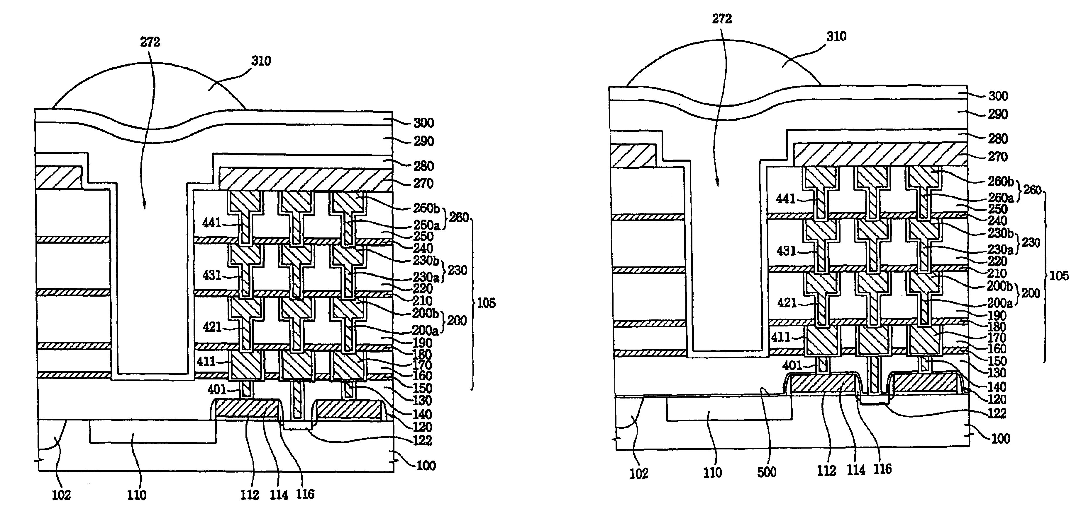
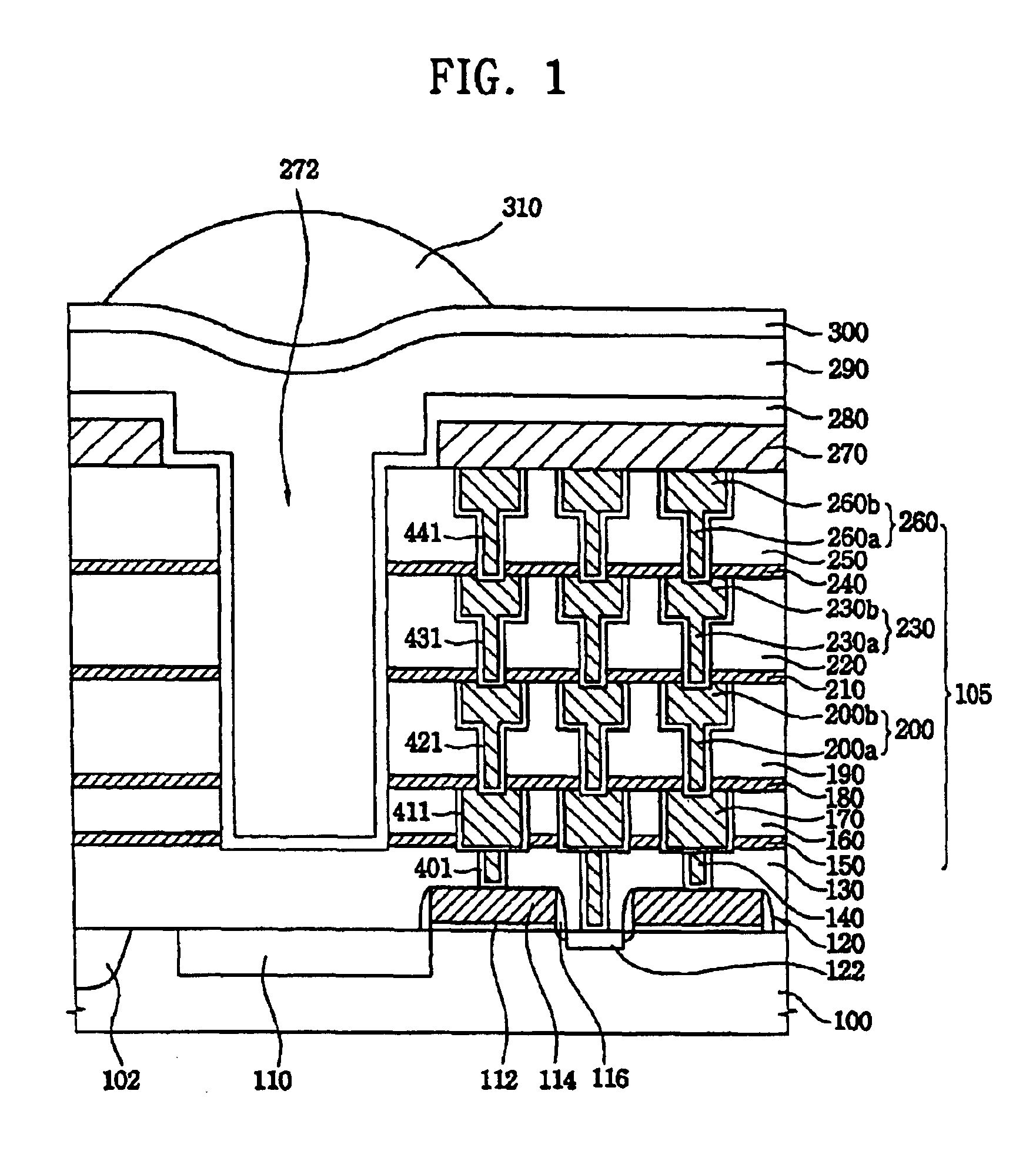
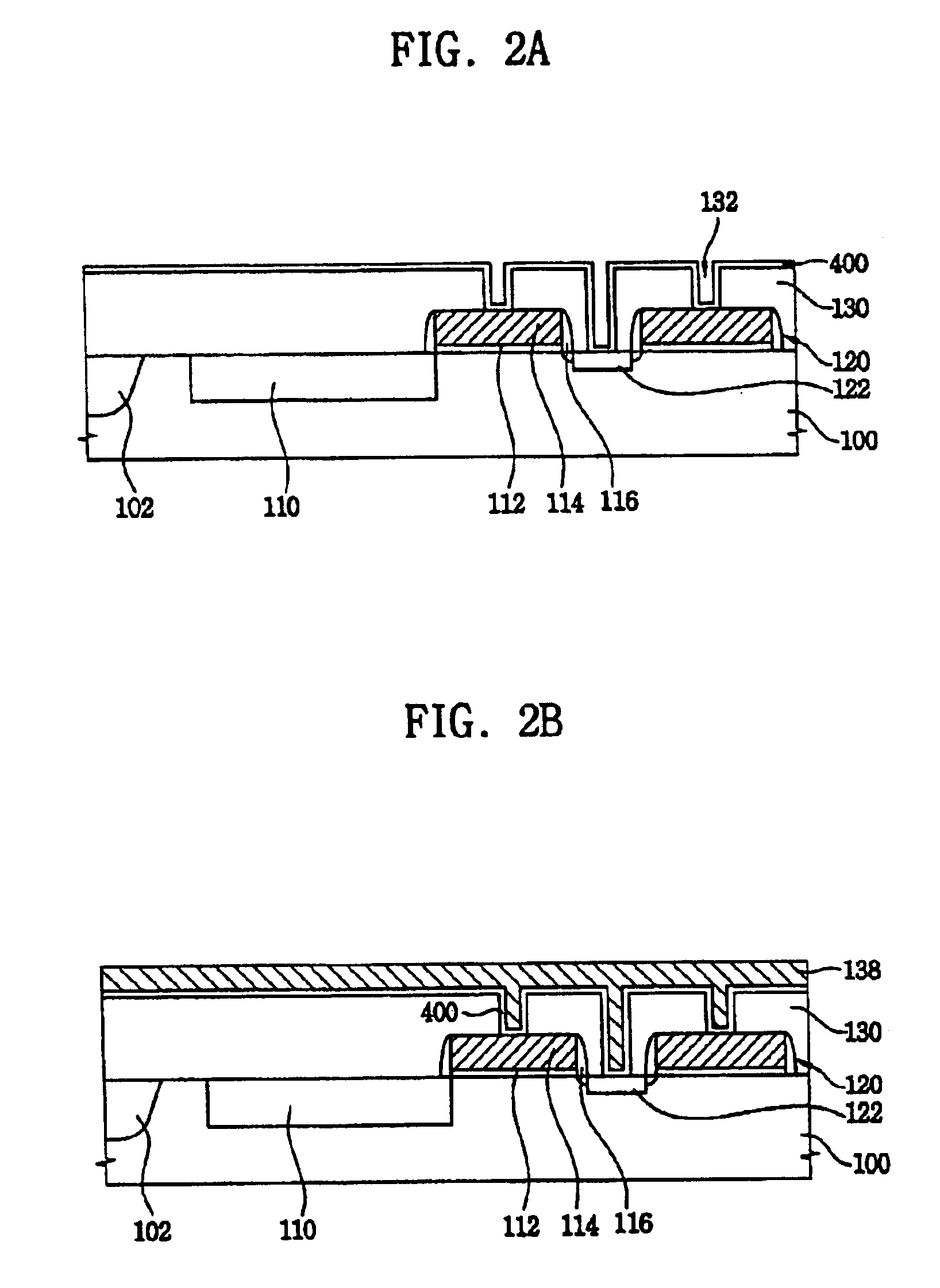
first embodiment
The remaining steps of forming the optional second protection layer 280, the transparent material 290, the color filter 300 and the lens 310, are the same as those for the first embodiment, and the resulting structure is illustrated in FIG. 4J.
third embodiment
the present invention is the same as the second embodiment, except in the formation of the dummy patterns. In the third embodiment, steps up to and including forming the via holes 308, dummy holes 303 and first interlayer dielectric dummy pattern 190′ are the same as in the second embodiment as illustrated in FIG. 6A.
However, in the third embodiment as illustrated in FIG. 6B, a photoresist pattern 304a is formed on the third interlayer dielectric layer 190 and the first interlayer dielectric dummy pattern 190′, to serve as a mask for etching the third interlayer dielectric layer 190 to form trenches 306. The first interlayer dielectric dummy pattern 190′ is not etched to a same depth as the trenches 306, as is the case in the second embodiment as shown in FIG. 4D.
second embodiment
In FIG. 6C, a third barrier metal layer 420b is formed on the third interlayer dielectric layer 190 and in dummy holes 303, trenches 306 and via holes 308, and a second copper layer 199b is then formed on the third barrier metal layer 420b to fill the dummy holes 303, the trenches 306 and the via holes 308. Then, as illustrated in FIG. 6D, the second copper layer 199b is planarized and portions of the second barrier metal layer 420b are removed in the same manner as that of the second embodiment to expose an upper surface of the third interlayer dielectric layer 190, and to form first interconnections 200 formed of trenches 200b and vias 200a, on a portion of barrier metal layer 421a and a second copper dummy pattern 312a on a portion of the barrier metal layer 423a.
Then, a second interlayer dielectric dummy pattern 220′, a third copper dummy pattern 322a, second interconnections 230 formed of trenches 230b and vias 230a, a third interlayer dielectric dummy pattern 250′, a third co...
PUM
 Abstract
Description
Claims
Application Information