Edge correction circuit

a technology of correction circuit and edge, applied in the field of edge correction circuit, can solve the problem that the necessary edge enhancement cannot be made adequately, and achieve the effect of optimizing the edge correction

Inactive Publication Date: 2005-03-08
MITSUBISHI ELECTRIC CORP
View PDF9 Cites 10 Cited by
  • Summary
  • Abstract
  • Description
  • Claims
  • Application Information

AI Technical Summary

Benefits of technology

The invention has been made to solve the problems described above, and its object is to provide an edge correcting circuit which can reduce or eliminate the overshoot, and which can fully achieve the necessary edge enhancement.
With the above arrangement, it is possible to adjust the overshoot components and the components improving the edge inclination independently of each other, so as to optimize the edge correction.

Problems solved by technology

It is possible to make the overshoot less prominent by reducing the high-frequency signal by the amplitude adjustment within the high-frequency extracting circuit 5, but in that case the necessary edge enhancement cannot be made adequately.

Method used


Image

  • Edge correction circuit
  • Edge correction circuit
  • Edge correction circuit

Examples


embodiment 1

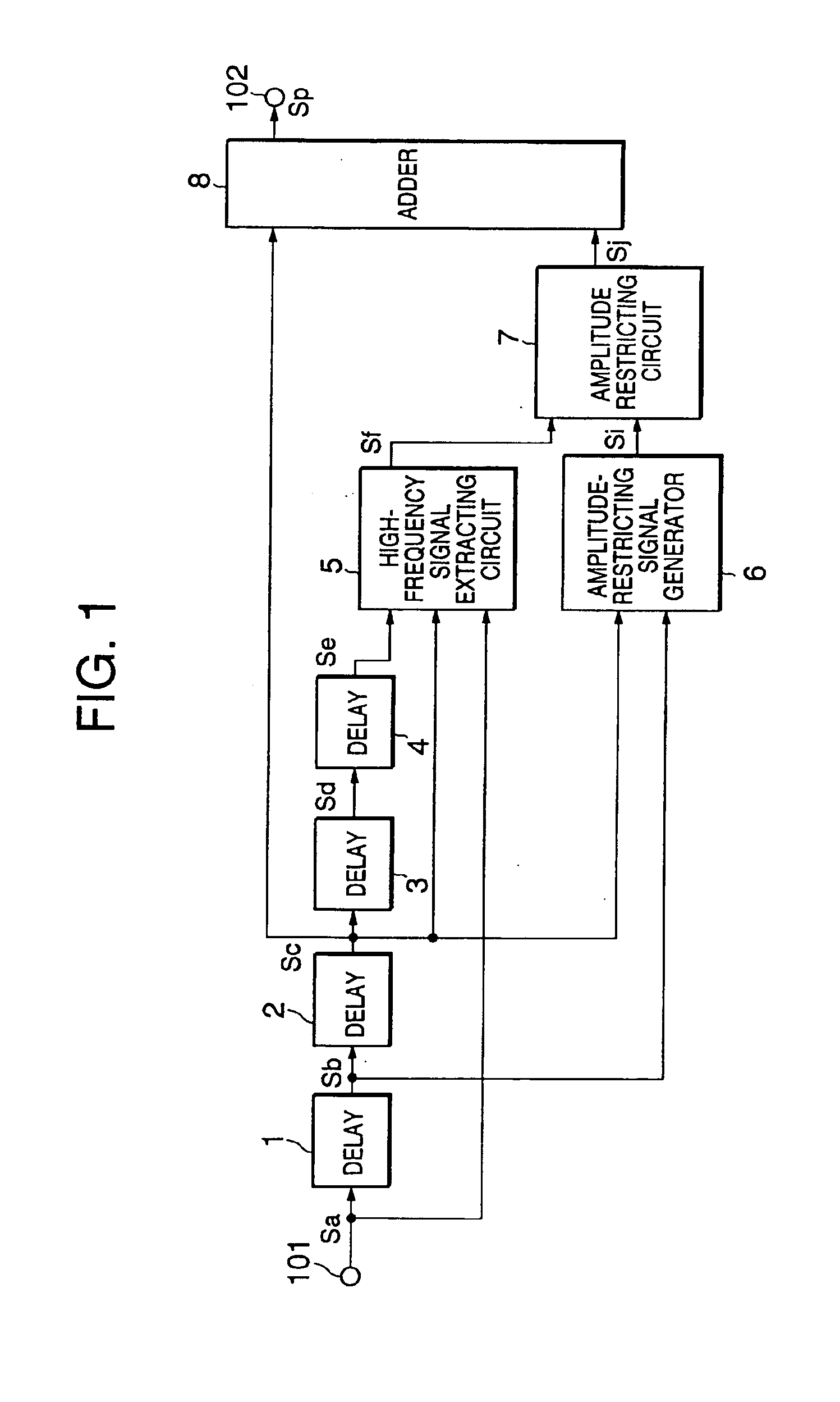
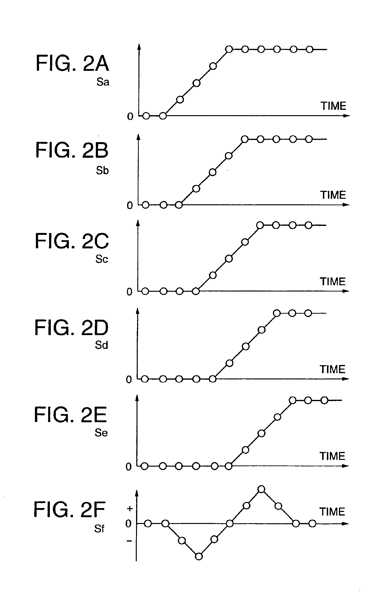
FIG. 1 is an edge correcting circuit of Embodiment 1 of the invention. FIGS. 2A to 2F, and FIGS. 3A to 3G show signals at various parts of the edge correcting circuit.

As shown in FIG. 1, the edge correcting circuit has an input terminal 101 for receiving a digitized image signal Sa formed of a sequence of digitized pixel signals representing luminance or colors of respective pixels, four one-pixel delay units 1, 2, 3 and 4 connected in series with each other, a high-frequency extracting circuit 5, an amplitude-restricting signal generator 6, an amplitude restricting circuit 7, an adder 8, and an output terminal 102 for outputting the edge-corrected image signal.

The image signal Sa input to the input terminal 101 is delayed successively by the one-pixel delay units 1, 2, 3 and 4 to become output signals Sb, Sc, Sd and Se (FIG. 2B, FIG. 2C, FIG. 2D and FIG. 2E) of the respective delay units.

The high-frequency extracting circuit 5 is formed of digital filters, and performs a predetermi...

embodiment 2

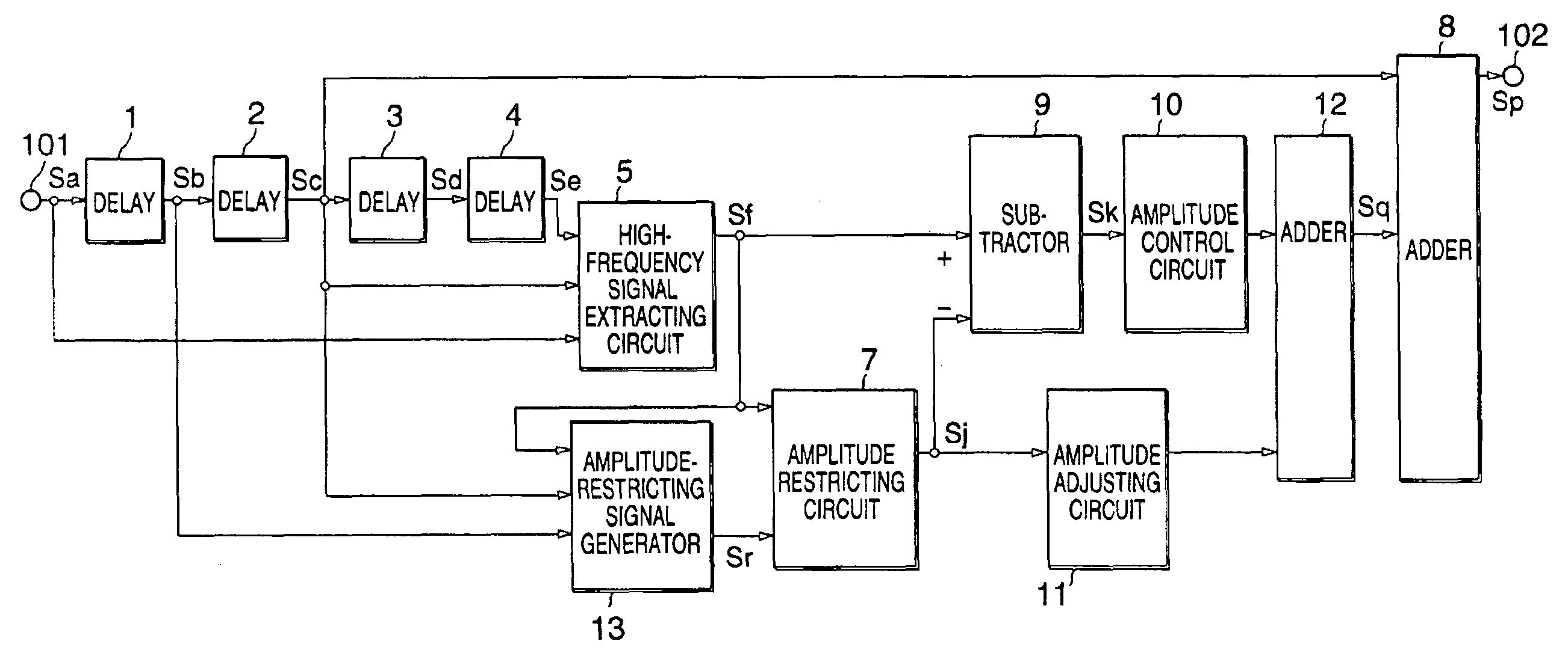
FIG. 7 is an edge-correcting circuit of Embodiment 2 of the present invention. Signals appearing at various parts of the circuit of this embodiment are shown in FIGS. 8A to 8H and FIGS. 2A to 2F. The edge correcting circuit of this embodiment is generally identical to that of Embodiment 1, but is different in additionally having a subtractor 9, an amplitude control circuit 10, an amplitude adjusting circuit 11, and an adder 12.

The subtractor 9 subtracts the inclination-improving signal Sj output from the amplitude restricting circuit 7, from the high-frequency signal Sf output from the high-frequency signal extracting circuit 5, to produce an overshoot signal Sk shown in FIG. 8G.

The amplitude control circuit 10 adjusts the amplitude of the overshoot signal Sk, and restricts the amplitude to within a predetermined value, by clipping. The amplitude adjusting circuit 11 adjusts the amplitude of the inclination-improving signal Sj output from the amplitude restricting circuit 7.

The adde...

embodiment 3

FIG. 9 shows an edge correcting circuit of Embodiment 3 of this invention. Signals appearing at various parts of the circuit of Embodiment 3 are shown in FIGS. 10A to 10G and FIGS. 2A to 2F. Embodiment 3 is generally identical to Embodiment 1, but the amplitude-restricting signal generator 6 of FIG. 1 is replaced by an amplitude-restricting signal generator 13.

The amplitude-restricting signal generator 13 differs from the amplitude-restricting signal generator 6 in that it receives the high-frequency signal Sf output from the high-frequency signal extracting circuit 5, in addition to the output signals Sb and Sc from the one-pixel delay units 1 and 2, and generates, therefrom, an amplitude-restricting signal Si for removing the overshoot components.

FIG. 11 shows details of the amplitude-restricting signal generator 13 of FIG. 9. In FIG. 11, reference numeral identical to those in FIG. 5 denote identical or corresponding members. As illustrated in FIG. 11, the amplitude-restricting s...


PUM


Abstract

In an edge correcting circuit of an image to be represented by a digitized image signal, a high-frequency signal extracting circuit (5) extracts a high-frequency signal of the image by calculation based on a signal of a target pixel, a signal of a pixel shifted from the target pixel by m (m being an integer not smaller than 2) pixels in the right or lower direction, and a signal of a pixel shifted from the target pixel by m pixels in the left or upper direction, an amplitude-restricting signal generator (6) determines an amplitude-restricting signal (Si) based on a minimum value or a maximum value of an absolute value of a difference between the signal of the target pixel and a signal of a pixel shifted from the target pixel by n (n being an integer not smaller than 1 and smaller than m) pixels in the right or lower direction, and an absolute value of a difference between the signal of the target pixel and a signal of a pixel shifted from the target pixel by n pixels in the left or upper direction, an amplitude restricting circuit (7) restricts the output of the high-frequency extracting circuit (5) to the output of the amplitude-restricting signal generator (6), and an adder (8) adds the output (Si) of the amplitude restricting circuit (7) or a signal obtained therefrom, as an edge correction signal (Sj, Sq), to the signal (Sc) of the target pixel. It is possible to obtain an edge-corrected image signal with the horizontal or vertical overshoots having been reduced or removed.

Description

BACKGROUND OF THE INVENTIONThe present invention relates to an edge correcting circuit for correcting the edge of the image represented by a digital image signal.In a display device used as a display terminal for a personal computer or a television set, edge correction by means of digital signal processing is adopted as a method for enhancing the edge of the displayed image to improve the sharpness. Generally, a high-frequency signal is extracted by passing the digital image signal through digital filters, and adding the high-frequency signal to the original signal, to obtain the edge-corrected image signal.FIG. 16 is a diagram showing a conventional edge correcting circuit. This edge correcting circuit comprises an input terminal 101 for receiving a digital image signal Sa, a one-pixel delay unit 1 for delaying the signal Sa by one pixel period to output a signal Sb, a one-pixel delay unit 2 for delaying the signal Sb by one pixel period to output a signal Sc, a one-pixel delay uni...

Claims


Application Information

Patent Timeline
Patent Type & Authority Patents(United States)
IPC IPC(8): H04N5/208H04N5/14G09G5/36
CPCH04N5/208H04N5/142
Inventor MINAMI, KOUJI
Owner MITSUBISHI ELECTRIC CORP
Why Eureka
Try Eureka