
Magnetic field sensor with augmented magnetoresistive sensing layer

Active Publication Date: 2005-03-29
NVE CORP
View PDF9 Cites 32 Cited by
  • Summary
  • Abstract
  • Description
  • Claims
  • Application Information

AI Technical Summary

Benefits of technology

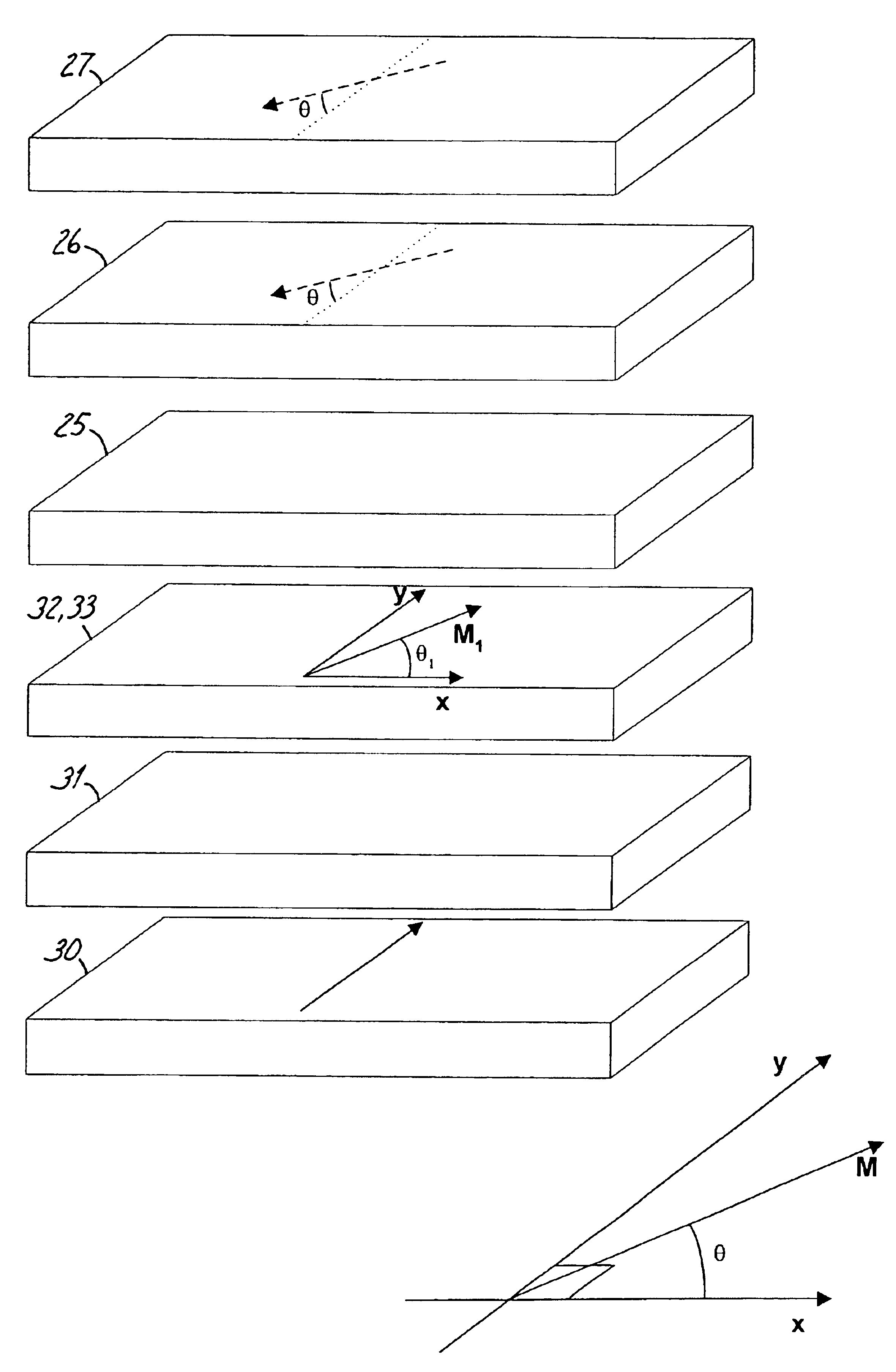
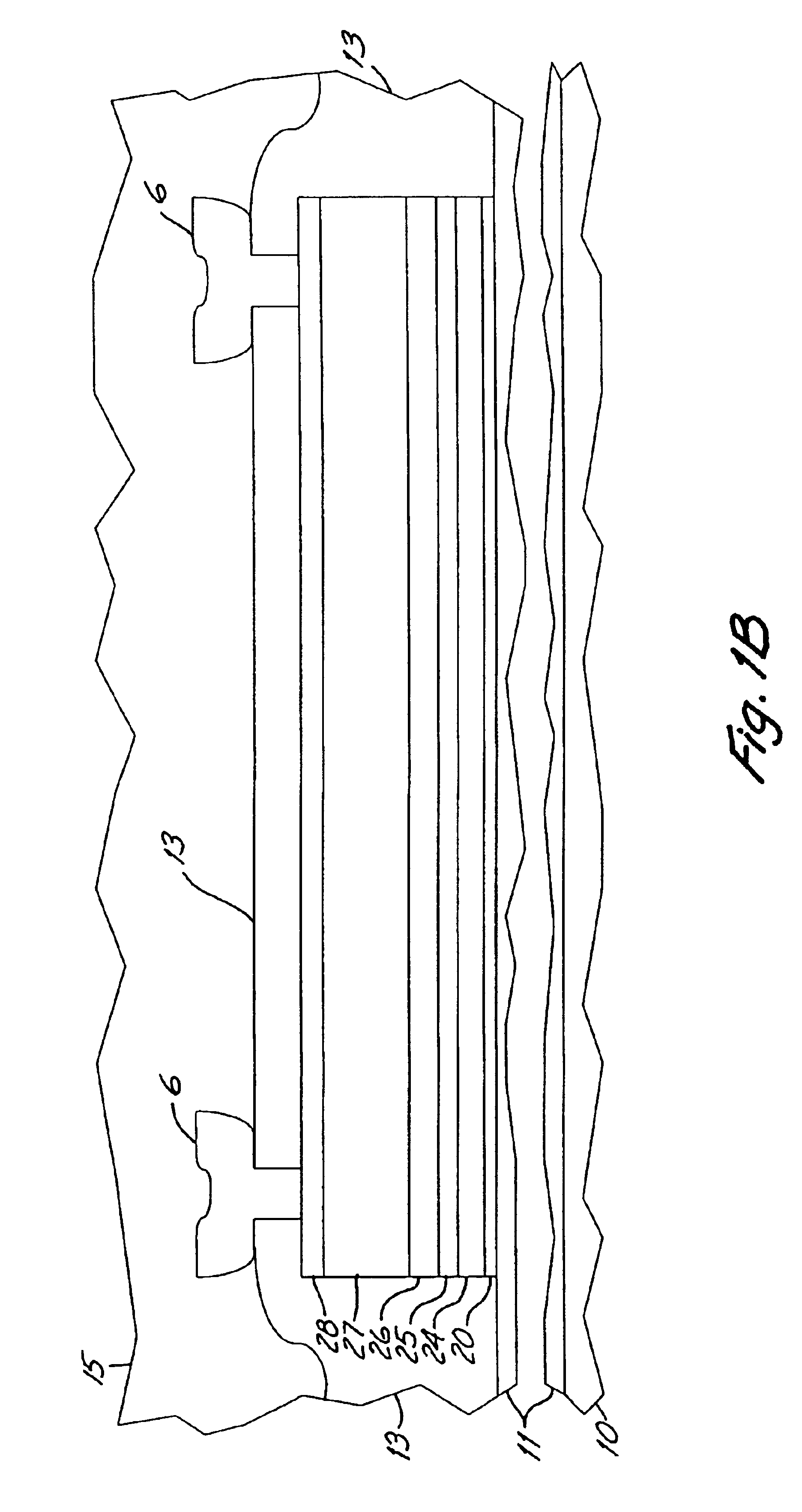
The present invention provides a ferromagnetic thin-film based magnetic field sensor with a sensing structure supported on a substrate having a nonmagnetic intermediate layer with two major surfaces on opposite sides thereof upon one of which a magnetization reference layer is provided. An anisotropic ferromagnetic material sensing layer is provided on that remaining one of the intermediate layer major surfaces. A spacer layer is provided on the sensing film and across this sensing film from one of the nonmagnetic intermediate layer major surfaces with the spacer layer having a major surface on a side thereof opposite the sensing film. An augmenting film of an anisotropic ferromagnetic material is provided on the spacer layer major surface with the spacer layer being sufficiently thick so as to significantly reduce or eliminate topological coupling between the sensing and augmenting films, and to significantly randomize spin states of emerging electrons traversing therethrough.

Problems solved by technology

The effect of the fringing fields from the pinned ferromagnetic material layer in such sensors detrimentally affects the external applied magnetic fields induced magnetization reversals of the free layer which causes a degradation in the linearity of its magnetoresistance versus applied external magnetic field characteristic, or linearity, of these sensors, and also an unwanted bias point shift of the free layer on such characteristics which limits the dynamic response range of the sensors.
The major challenges in making linear spin-valve sensors are to reduce the hysteresis and optimize the bias point.
However, all such measures complicate the fabrication process and usually lead to the resulting sensor consuming an undue amount of electrical power.

Method used


Image

  • Magnetic field sensor with augmented magnetoresistive sensing layer
  • Magnetic field sensor with augmented magnetoresistive sensing layer
  • Magnetic field sensor with augmented magnetoresistive sensing layer

Examples


Embodiment Construction

Two important aspects of the present invention enabling reduced hysteresis are 1) the pinning of the pinned layer in a direction at an angle relative to the direction of the magnetoresistor length so that a component of the interlayer coupling between the free and pinned layers can provide a bias to the free layer along the magnetoresistor length, and 2) to employ a spin-valve sensor having an augmenting second free ferromagnetic material layer. The present invention not only effectively reduces the sensor hysteresis in the sensor magnetoresistance versus applied external magnetic field characteristic but also provide a means to adjust and optimize the bias point of the linear spin-valve sensor on that characteristic. In the present invention, the spin-valve sensor is provided with a second free ferromagnetic material layer as contrasted with the usual single free layer. One of these free layers is the sensing layer which contributes to the sensor giant magnetoresistive effect respo...


PUM

PropertyMeasurementUnit
Fractionaaaaaaaaaa
Fractionaaaaaaaaaa
Fractionaaaaaaaaaa

Abstract

A ferromagnetic thin-film based magnetic field sensor having a nonmagnetic intermediate layer with two major surfaces on opposite sides thereof upon one of which a magnetization reference layer is provided and upon the other there being provided a sensing layer. A spacer layer is provided on the sensing film to separate this sensing film from an augmenting film with the spacer layer being sufficiently thick so as to significantly reduce or eliminate topological coupling between the sensing and augmenting films, and to significantly randomize spin states of emerging electrons traversing therethrough.

Description

BACKGROUND OF THE INVENTIONThe present invention relates to low hysteresis exchange biased spin-valve and spin dependent tunneling magnetic field sensors.Many kinds of electronic systems make use of magnetic material based devices. Digital memories are used extensively in digital systems of many kinds including computers and computer systems components, and digital signal processing systems. Such memories can be advantageously based on the storage of digital bits as alternative states of magnetization in magnetic materials in each memory cell, particularly in cells using thin-film magnetic materials, resulting in memories which use less electrical power and do not lose information upon removals of such electrical power.Magnetometers and other magnetic sensing devices are also used extensively in many kinds of systems including magnetic disk memories and magnetic tape storage systems of various kinds. Such devices provide output signals representing the magnetic fields sensed thereby...

Claims


Application Information

Patent Timeline
IPC IPC(8): G01R33/06G01R33/09G11B5/39
CPCB82Y10/00H01F10/3295G01R33/093G11B5/3906G11B5/3909G11B5/3935G11B5/398H01F10/3272H01L43/08B82Y25/00G11B2005/3996H01F10/3254Y10T428/12646Y10T428/1121Y10T428/1171Y10T428/12806Y10T428/32Y10T428/2495Y10T428/12986Y10T428/12465H10N50/10
Inventor QIAN, ZHENGHONGDAUGHTON, JAMES M.WANG, DEXINTONDRA, MARK C.
Owner NVE CORP
Learn More