Semiconductor device and a method of manufacturing the same, a circuit board and an electronic apparatus

a technology of semiconductor devices and electronic devices, which is applied in the direction of mechanical devices, valve member-seat contacts, basic electric elements, etc., can solve the problems of difficult formation of insulating layers on the inner face of small through holes and difficult formation of insulating layers

Inactive Publication Date: 2005-03-29
ADVANCED INTERCONNECT SYST LTD
View PDF3 Cites 231 Cited by
  • Summary
  • Abstract
  • Description
  • Claims
  • Application Information

AI Technical Summary

Problems solved by technology

In this case, it has been difficult to form the insulating layer on the inner face of the small through hole and to form the conductive electrode inside the insulating layer.

Method used


Image

  • Semiconductor device and a method of manufacturing the same, a circuit board and an electronic apparatus
  • Semiconductor device and a method of manufacturing the same, a circuit board and an electronic apparatus
  • Semiconductor device and a method of manufacturing the same, a circuit board and an electronic apparatus

Examples


Embodiment Construction

The embodiment of the present invention resolves the above conventional problems and is intended for forming the through electrode with ease.

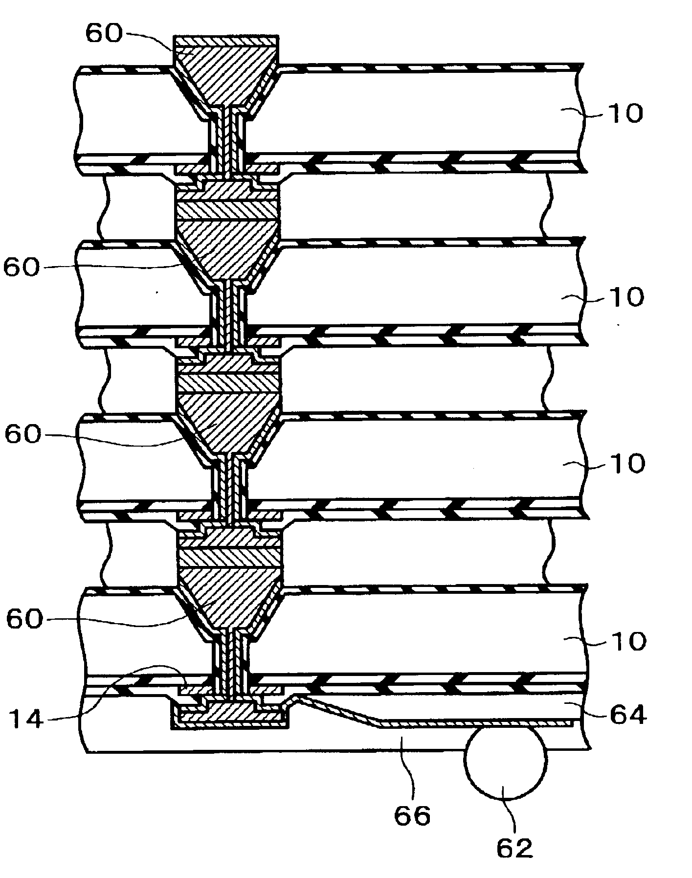
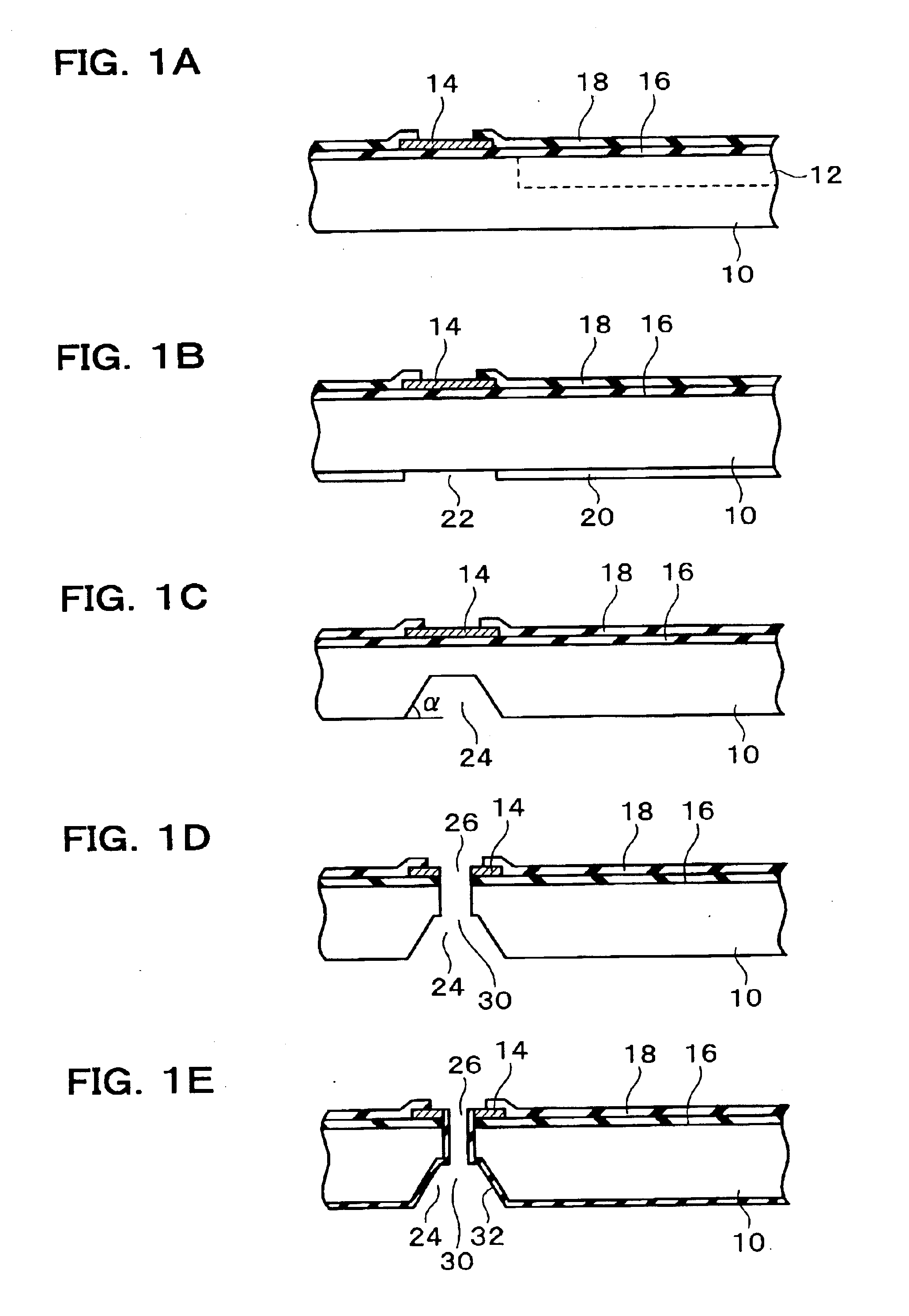
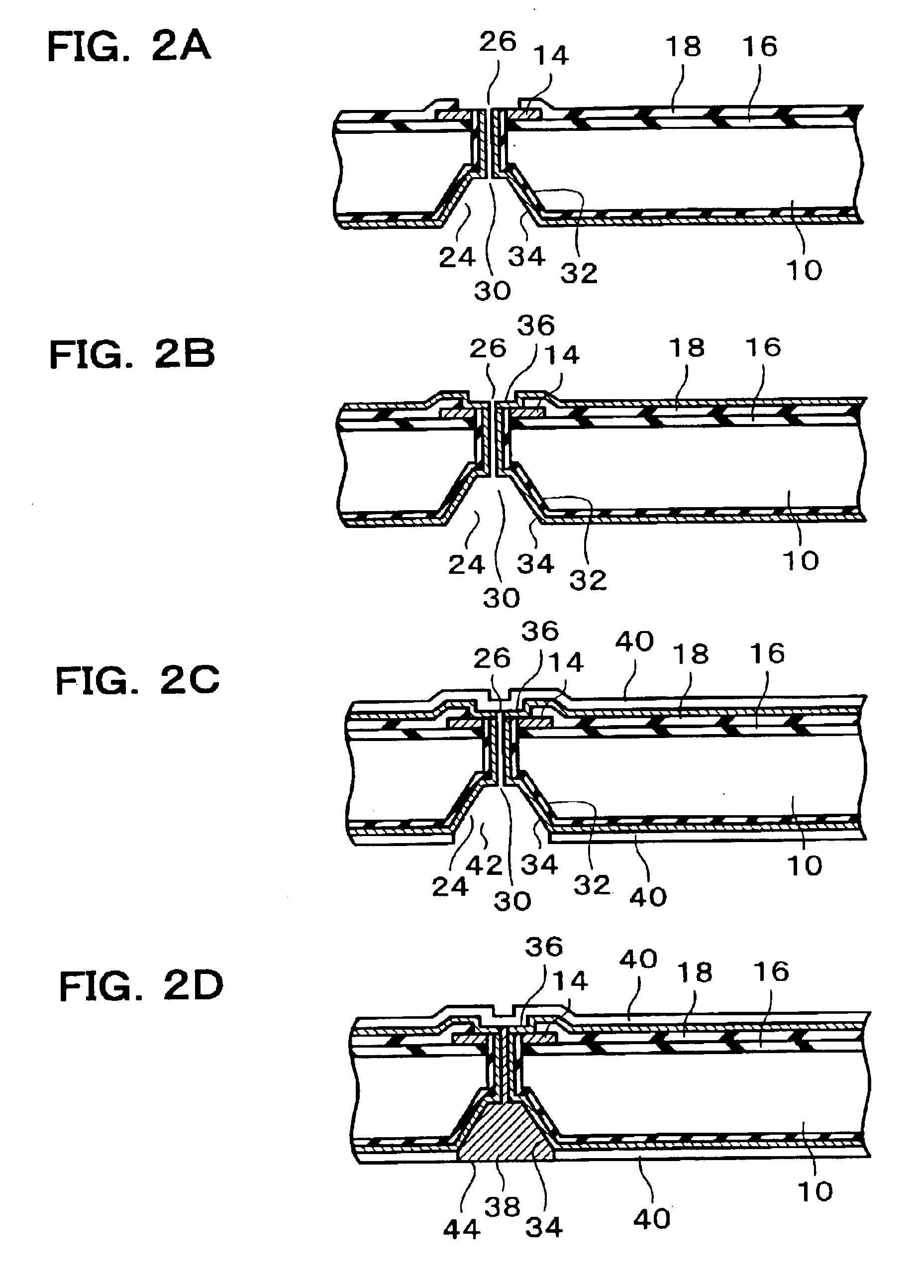
(1) A semiconductor device manufacturing method according to an embodiment of the present invention comprises:(a) forming a through hole tapered from an opening to an in-depth direction in a semiconductor substrate provided with an integrated circuit;(b) forming an insulating layer on an inner surface of the through hole by supplying an insulating material to the through hole through the opening; and(c) forming a conductive portion inside the insulating layer by supplying a conductive material through the opening to the through hole provided with the insulating layer.

According to an embodiment of the invention, since the opening of the through hole is open wide, and it is easy to supply the insulating material and the conductive material, a through electrode can easily be formed.

(2) In the semiconductor device manufacturing method, the through ...


PUM


Abstract

A through hole tapered from an opening to the in-depth direction is formed in a semiconductor substrate provided with an integrated circuit. An insulating material is supplied to the through hole through the opening so as to form an insulating layer on the inner surface of the through hole. A conductive material is supplied through the opening to the through hole provided with the insulating layer so as to form a conductive portion inside the insulating layer.

Description

BACKGROUND OF THE INVENTIONThe present invention relates to a semiconductor device and a method of manufacturing the same, a circuit board and an electronic apparatus.Three-dimensionally mounted semiconductor devices are being developed. Further, in an attempt to realize the three-dimensional mounting, forming a through electrode in, a semiconductor chip is well known. More specifically, a through hole is formed in the semiconductor chip, and an insulating layer is formed on the inner face of the through hole. The through electrode is then formed inside the insulating layer. In this case, it has been difficult to form the insulating layer on the inner face of the small through hole and to form the conductive electrode inside the insulating layer.BRIEF SUMMARY OF THE INVENTIONA semiconductor device manufacturing method according to an aspect of the present invention comprises:(a) forming a through hole tapered from an opening to an in-depth direction in a semiconductor substrate prov...

Claims


Application Information

Patent Timeline
Patent Type & Authority Patents(United States)
IPC IPC(8): H01L21/70H01L25/065H01L21/60H01L21/02H01L23/12H01L23/48H01L21/768H01L21/3205H01L31/0264H01L25/07H01L25/18H01L31/0328H01L23/52H01L21/268H01L23/31H01L23/485
CPCH01L21/268H01L21/76898H01L24/13H01L23/3114H01L23/481H01L24/10H01L25/0657H01L2224/13099H01L2924/01004H01L2924/01013H01L2924/01027H01L2924/01029H01L2924/01033H01L2924/01078H01L2924/14H01L2924/19043H01L2924/01005H01L2924/01006H01L2924/014H01L2225/06513H01L2225/06541H01L2225/06565H01L2924/00H01L24/05H01L2224/05001H01L2224/05009H01L2224/05025H01L2224/05027H01L2224/05548H01L2224/06181H01L2224/13H01L2224/13009H01L2224/14181H01L2924/00014H01L2924/12042H01L2224/05599H01L2224/05147F16K1/22F16K25/005F16K37/00
Inventor MIYAZAWA, IKUYAIKEHARA, TADAYOSHI
Owner ADVANCED INTERCONNECT SYST LTD
Why Eureka
Try Eureka