Eureka AIR delivers breakthrough ideas for toughest innovation challenges, trusted by R&D personnel around the world.

Thin lightshield process for solid-state image sensors

a technology of solid-state image sensors and lightshields, applied in the direction of material analysis, instruments, radiation control devices, etc., can solve the problems of degrading performance, corrosion of these films, electrical properties or optical light-shielding properties, etc., and achieve the effect of thin lightshields and minimizing corrosion of aluminum and tiw layers

Active Publication Date: 2005-04-12
OMNIVISION TECH INC
View PDF3 Cites 3 Cited by
  • Summary
  • Abstract
  • Description
  • Claims
  • Application Information

AI Technical Summary

Benefits of technology

The present invention is an image sensor that solves problems associated with previous image sensors. It includes a substrate with photosensitive areas, an insulator spanning the substrate, and a multi-layer metallization structure consisting of two layers. The first layer forms light shield regions, circuit interconnections, and barrier regions to prevent spiking into the substrate or gates at contacts in the non-imaging area. The second layer spans the interconnections and barrier regions of the first layer only over the non-imaging areas and overlaps the edges of the first layer. This structure improves the image sensor's performance and reliability.

Problems solved by technology

Regions are protected from light because light absorbed in these protected regions causes degraded performance through mechanisms such as color crosstalk, smear, or reduced blooming control.
Further, this residue may react with the aluminum or TiW, especially where the aluminum and TiW meet, causing corrosion of these films, and degradation of their electrical properties or optical light-shielding properties.
This requirement may restrict the use of certain metals for the bi-layer metallization.

Method used


Image

  • Thin lightshield process for solid-state image sensors
  • Thin lightshield process for solid-state image sensors
  • Thin lightshield process for solid-state image sensors

Examples


Embodiment Construction

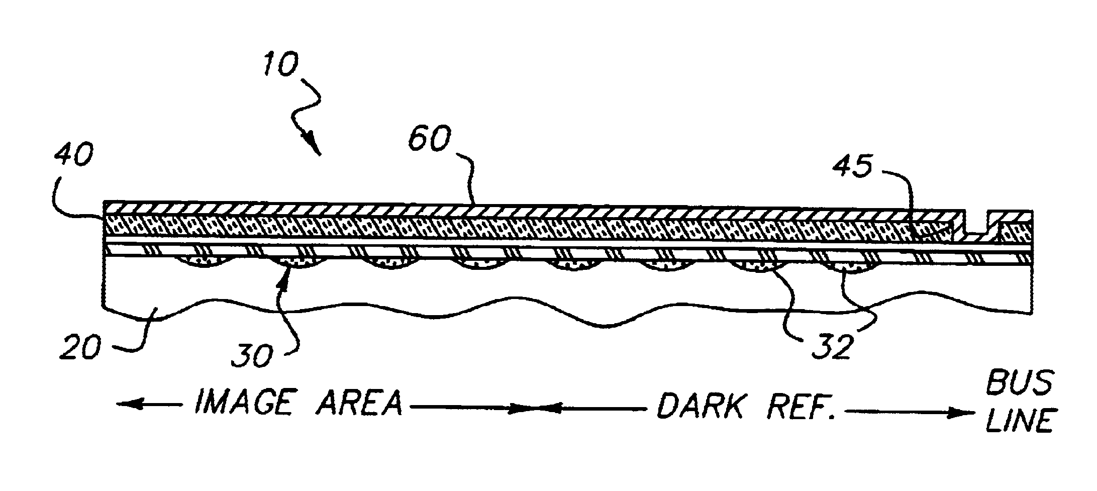
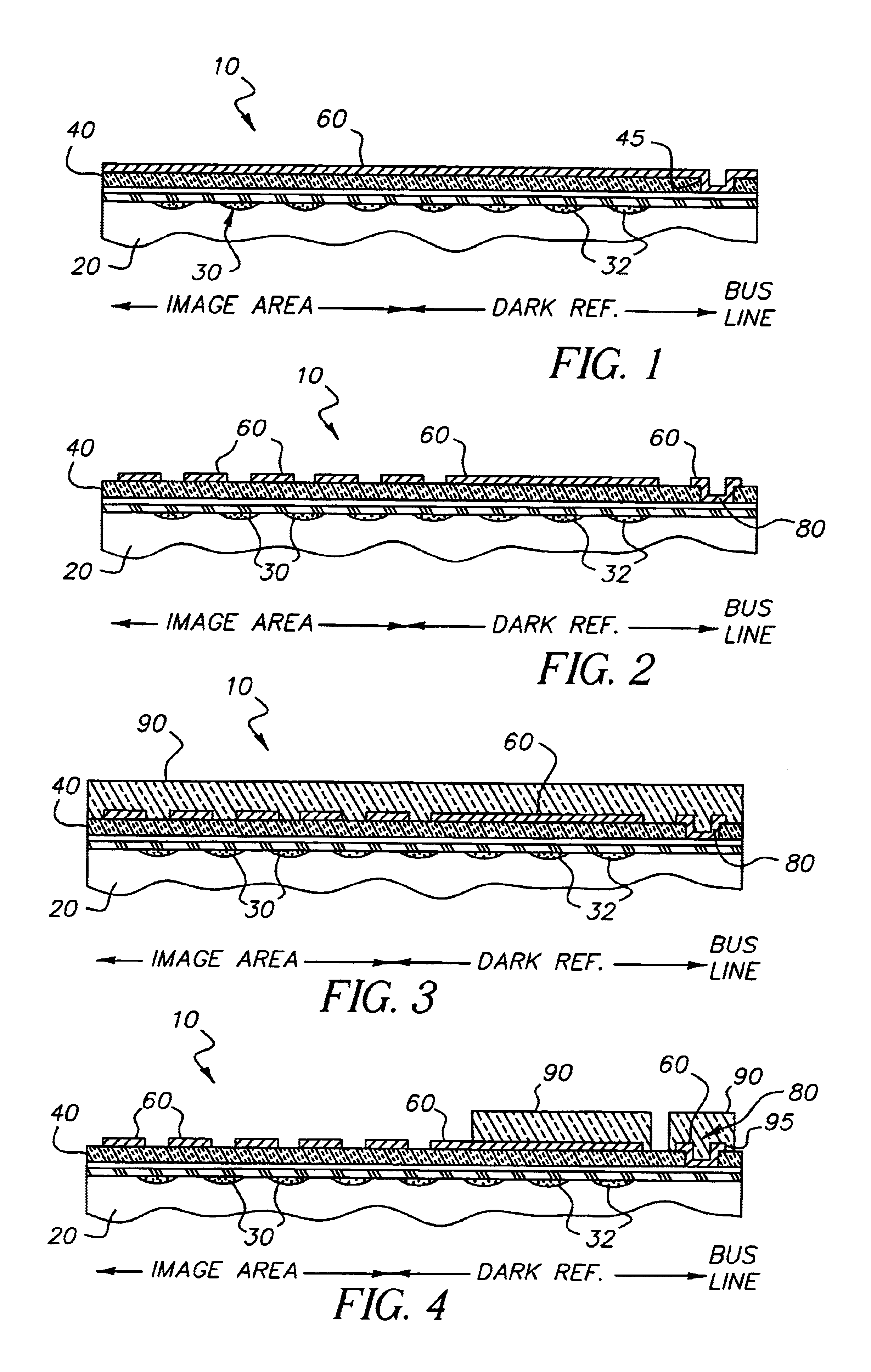
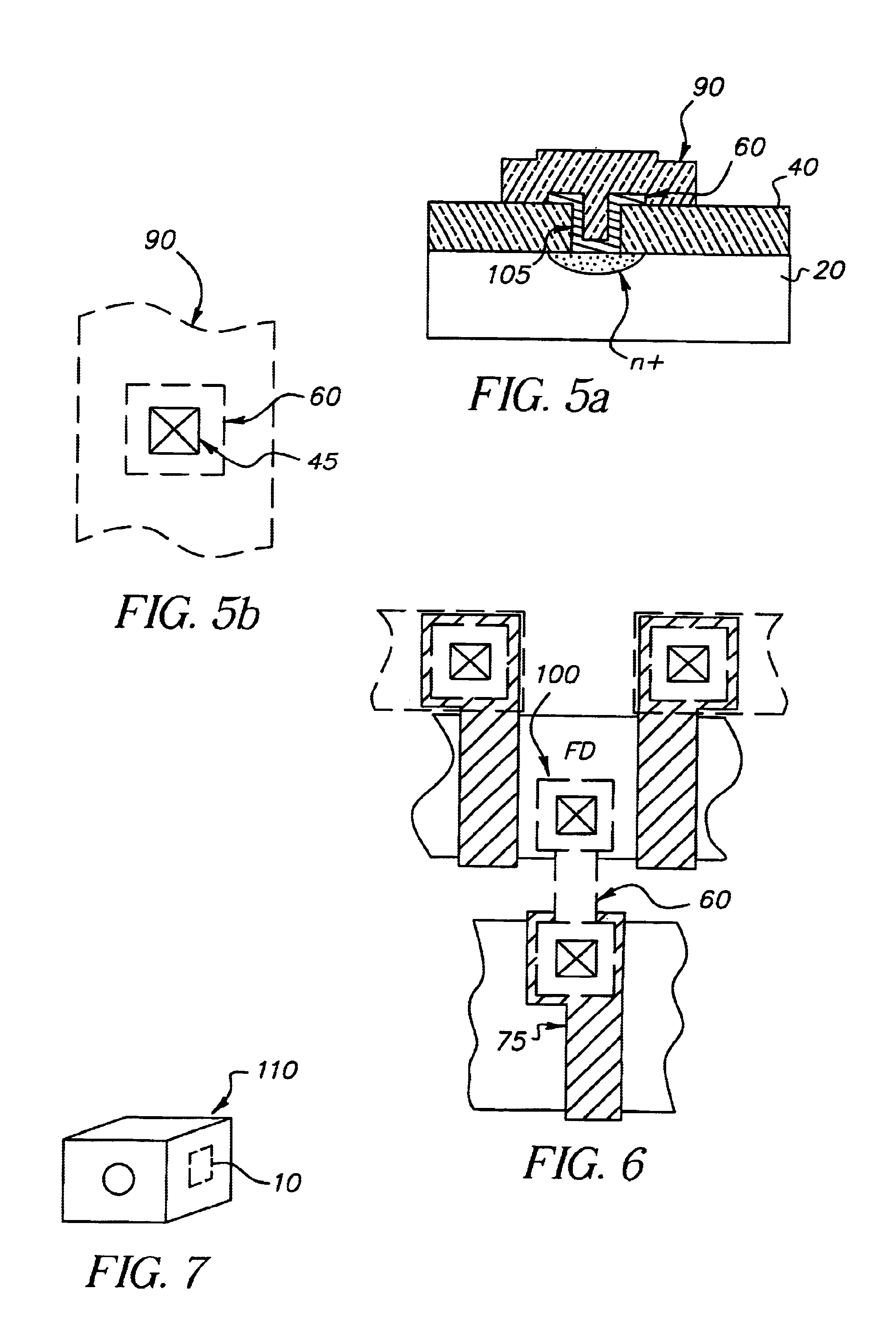
Referring to FIG. 1, a typical image sensor 10 consists of an array of photosensitive elements or pixels 30 in an image area. Within each pixel are regions that are exposed to light so that an electrical signal may be created in response to the incident light. In addition, there are regions within the pixel, which are prevented from receiving light because the light will degrade the imaging performance. A typical image sensor 10 also provides dark reference pixels 32 that are insensitive to light because they are covered with a light shield. The signal from these dark reference pixels 32 are used in the signal processing portion of the camera to indicate the signal of photosensitive pixels when no light is incident upon them. In addition, interconnects are provided within the image sensor to electrically connect various parts of the imager and to provide means to connect the imager to external circuits.

Referring to FIG. 1, there is shown an initial stage of forming an image sensor 1...


PUM


Abstract

An image sensor includes a substrate having photosensitive areas; an insulator spanning the substrate; and a first and second layer of a multi-layer metallization structure, wherein the first layer forms light shield regions over selected portions of the photosensitive area as well forming circuit interconnections and barrier regions to prevent spiking into the substrate or gates at contacts in the non-imaging area; and the second layer spanning the interconnections and barrier regions of the first layer only over the non-imaging areas and the second layer overlays edges of the first layer.

Description

FIELD OF THE INVENTIONThe invention relates generally to the field of solid-state image sensors, and more particularly to the process of forming a lightshield and the interconnection layers for a solid-state image sensor.BACKGROUND OF THE INVENTIONImage sensors are made of an array of pixels. Within each pixel, some regions are specifically designed to be photosensitive, and other regions are protected from light by a lightshield. Regions are protected from light because light absorbed in these protected regions causes degraded performance through mechanisms such as color crosstalk, smear, or reduced blooming control.In U.S. patent application Ser. No. 10 / 641,724, filed Aug. 15, 2003, entitled “Light Shield Process For Solid-State Image Sensors,” by Eric G. Stevens, a thin lightshield process is described for providing a lightshield from one of the layers of a bi-layer metallization process. The aluminum layer in this process is usually patterned with a chlorine-based plasma chemist...

Claims


Application Information

Patent Timeline
Patent Type & Authority Patents(United States)
IPC IPC(8): H01L21/00H01L21/4763H01L21/02H01L31/02H01L27/146
CPCH01L27/14623H01L27/14685H01L27/14636
Inventor NICHOLS, DAVID N.STEVENS, ERIC G.KOSMAN, STEPHEN L.
Owner OMNIVISION TECH INC
Why Eureka
Eureka Blog
Learn More