Multiple die interconnect system

a multi-die assembly and interconnection technology, applied in the direction of solid-state devices, basic electric elements, electrical apparatus construction details, etc., can solve the problems of difficult and expensive fabrication of vias 70 and achieve the effect of low impedance signals

Inactive Publication Date: 2005-04-19
FORMFACTOR INC
View PDF5 Cites 99 Cited by
  • Summary
  • Abstract
  • Description
  • Claims
  • Application Information

AI Technical Summary

Benefits of technology

[0014]The claims portion of this specification particularly points out and distinctly claims the subject matter of the invention. However those skilled in the art will best understand both the organization and method of operation of what the applicant(s) consider to be the best mode(s) of practicing the invention, together with further advantages and objects of the invention, by reading the remaining portions of the specification in view of the accompanying drawing(s) wherein like reference characters refer to like elements.

Problems solved by technology

However vias 70 are difficult and expensive to fabricate.

Method used


Image

  • Multiple die interconnect system
  • Multiple die interconnect system
  • Multiple die interconnect system

Examples


Embodiment Construction

[0032]The present invention is directed to multiple die assemblies, and this specification describes several exemplary embodiments and applications of the invention. However the invention is not limited to these exemplary embodiments and applications or to the particular manner in which the exemplary embodiments and applications operate or are described herein.

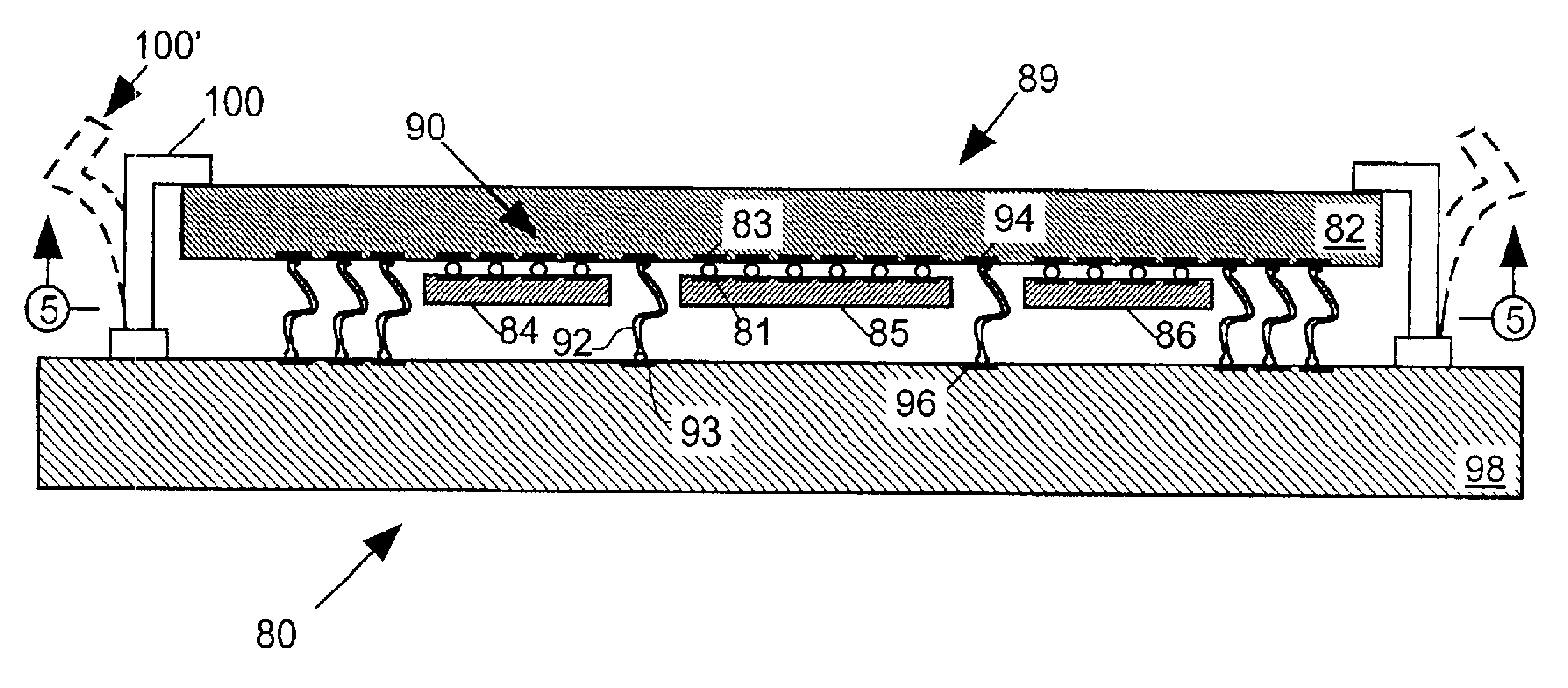
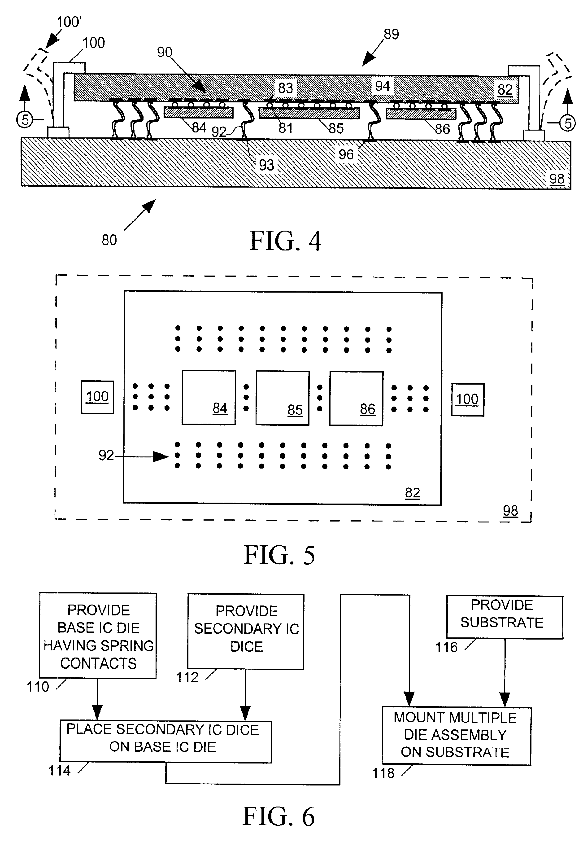
[0033]FIG. 4 is a sectional elevation view of an interconnect system 80 in accordance with an exemplary embodiment of the invention for providing signal paths between a multiple die assembly 89 and a substrate 98. FIG. 5 is a sectional plan view along cut line 5—5 of FIG. 4. In the preferred embodiment of the invention, substrate 98 is a printed circuit board (PCB) for holding integrated circuit or other devices (not shown) that are to communicate with circuits implemented within multiple die assembly 89. However substrate 98 may be any other kind of substrate for holding devices such as, for example, a semiconductor substrate...


PUM

PropertyMeasurementUnit
conductiveaaaaaaaaaa
frequencyaaaaaaaaaa
speedaaaaaaaaaa

Abstract

A multiple integrated circuit (IC) die assembly includes a base IC die and secondary IC dice mounted on a surface of the base IC die. A set of protruding contacts formed on the surface of the base IC die and extending beyond the secondary IC dice link the surface of the base IC die to a printed circuit board (PCB) substrate with the secondary IC die residing between the base IC die and the PCB substrate.

Description

BACKGROUND OF THE INVENTION[0001]1. Field of the Invention[0002]The present invention relates to a system for interconnecting a multiple die assembly to a printed circuit board or other substrate.[0003]2. Description of Related Art[0004]FIG. 1 is a simplified sectional elevation view of a prior art multiple die electrical system 10 including a multiple die assembly 12 mounted on a printed circuit board (PCB) or other substrate 14. Multiple die assembly 12 includes a set of secondary dice 16-18 mounted directly on a base die 20 within an integrated circuit (IC) package 28. Solder 22 conductively links bond pads 24 on dice 16-18 to bond pads 26 on die 20. An IC socket 36 mounted on substrate 14 releasably secures and interconnects each package pin 34 through a contact 37 and a solder ball 38 to one of a set of traces 39 on PCB 14. Bond wires 30 link various bond pads 32 on base die 20 to package pins 34. For illustration purposes solder 22 is shown much thicker than it would be after ...

Claims


Application Information

Patent Timeline
Patent Type & Authority Patents(United States)
IPC IPC(8): H01L25/065H01L23/52H01L23/13H01L23/538H01L23/498H01L23/12H01L23/48H05K7/10H01L25/18H01L25/07
CPCH01L23/13H01L23/5385H01L25/0652H05K7/1092H01L23/49811Y10T29/53178H01L2224/1134H01L2224/13099H01L2224/16H01L2924/01078H01L2924/15312H01L2924/1532H01L2924/16152H01L2924/3011Y10T29/49126Y10T29/49149Y10T29/4913H01L2924/00013H01L2924/01019H01L2924/19107H01L2224/16225Y10T29/49147Y10T29/53174H01L2924/00014H01L2224/05571H01L2224/05573H01L2224/05599H01L23/48
Inventor MILLER, CHARLES A.
Owner FORMFACTOR INC
Why Eureka
Try Eureka