Methods and apparatus for improving resolution and reducing the effects of signal coupling in an electronic imager

a technology of electronic imager and signal coupling, which is applied in the field of electronic imager, can solve the problems of charge sharing being a more significant problem and affecting image quality, and achieve the effects of reducing signal coupling effects, improving image resolution, and simple and fast imaging

Inactive Publication Date: 2005-04-26
MASSACHUSETTS INST OF TECH
View PDF7 Cites 2 Cited by
  • Summary
  • Abstract
  • Description
  • Claims
  • Application Information

AI Technical Summary

Benefits of technology

[0011]With this arrangement, a relatively simple and fast imaging circuit is provided which reduces the effects of signal coupling and improves image resolution by the use of sub-pixels in the generated image. These advantages are achieved in the imager read out apparatus itself, rather than in a post-processor, thereby permitting substantially “real-time” processing and reducing or eliminating post-processor requirements and the need for storage of the read out signals for subsequent post-processing. Further, the simplicity of the circuitry permits large numbers of detector output signals to be processed without concern for post-processor computational capability and capacity.

Problems solved by technology

When a signal couples to more than one imager channel or a signal from one channel couples to another channel, image quality can be adversely affected.
Charge sharing can be a more significant problem in systems in which a signal processing function is performed on the detector output signals.

Method used


Image

  • Methods and apparatus for improving resolution and reducing the effects of signal coupling in an electronic imager
  • Methods and apparatus for improving resolution and reducing the effects of signal coupling in an electronic imager
  • Methods and apparatus for improving resolution and reducing the effects of signal coupling in an electronic imager

Examples


Embodiment Construction

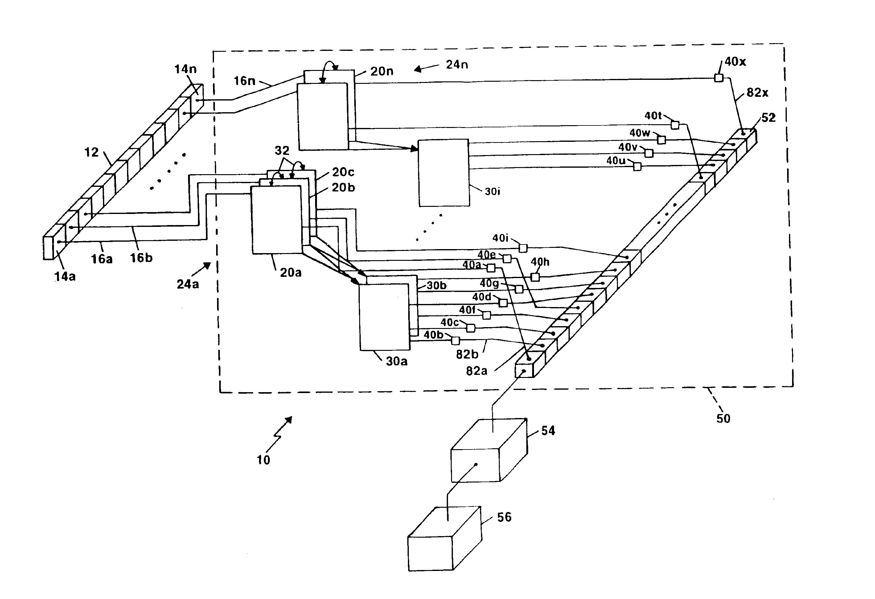
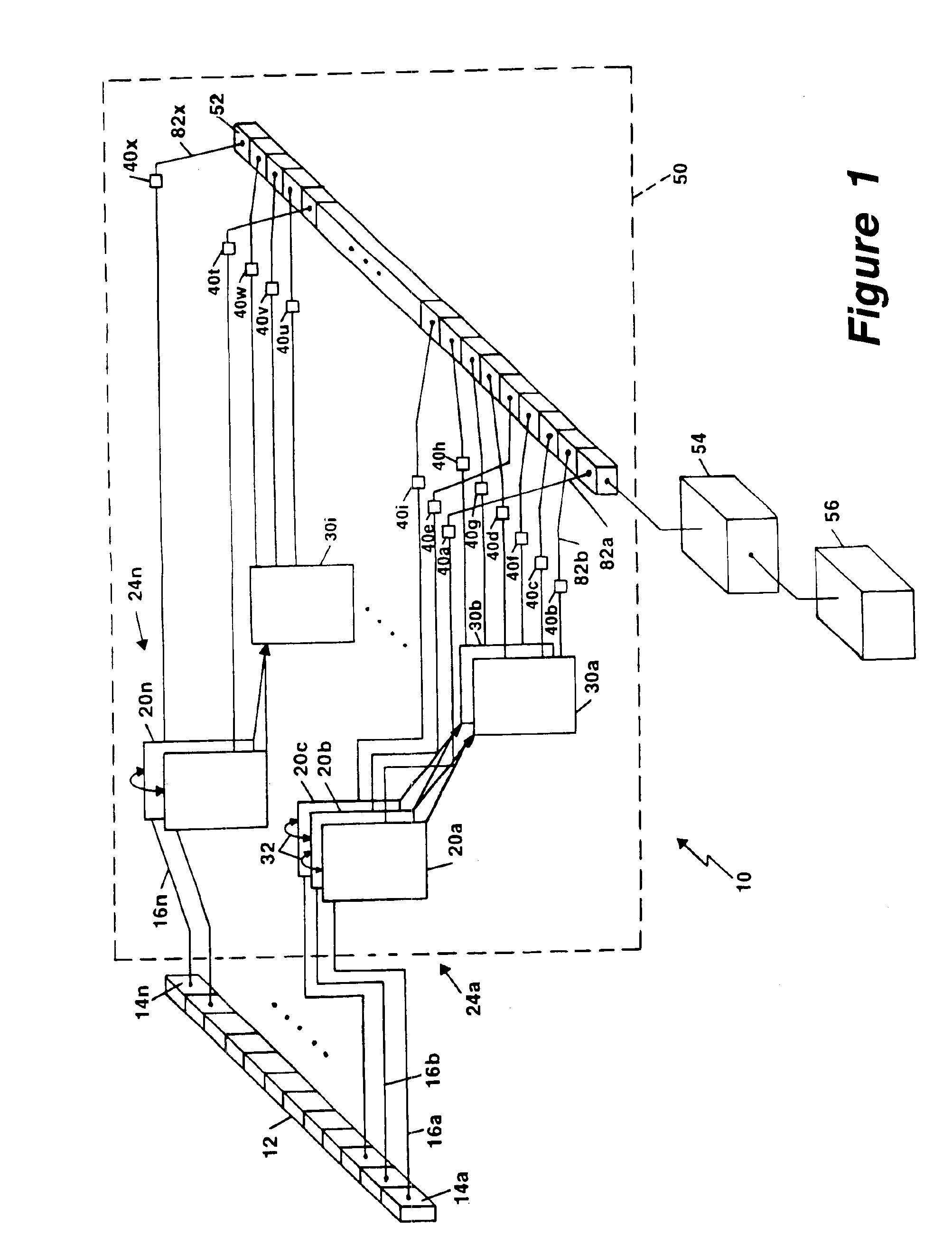
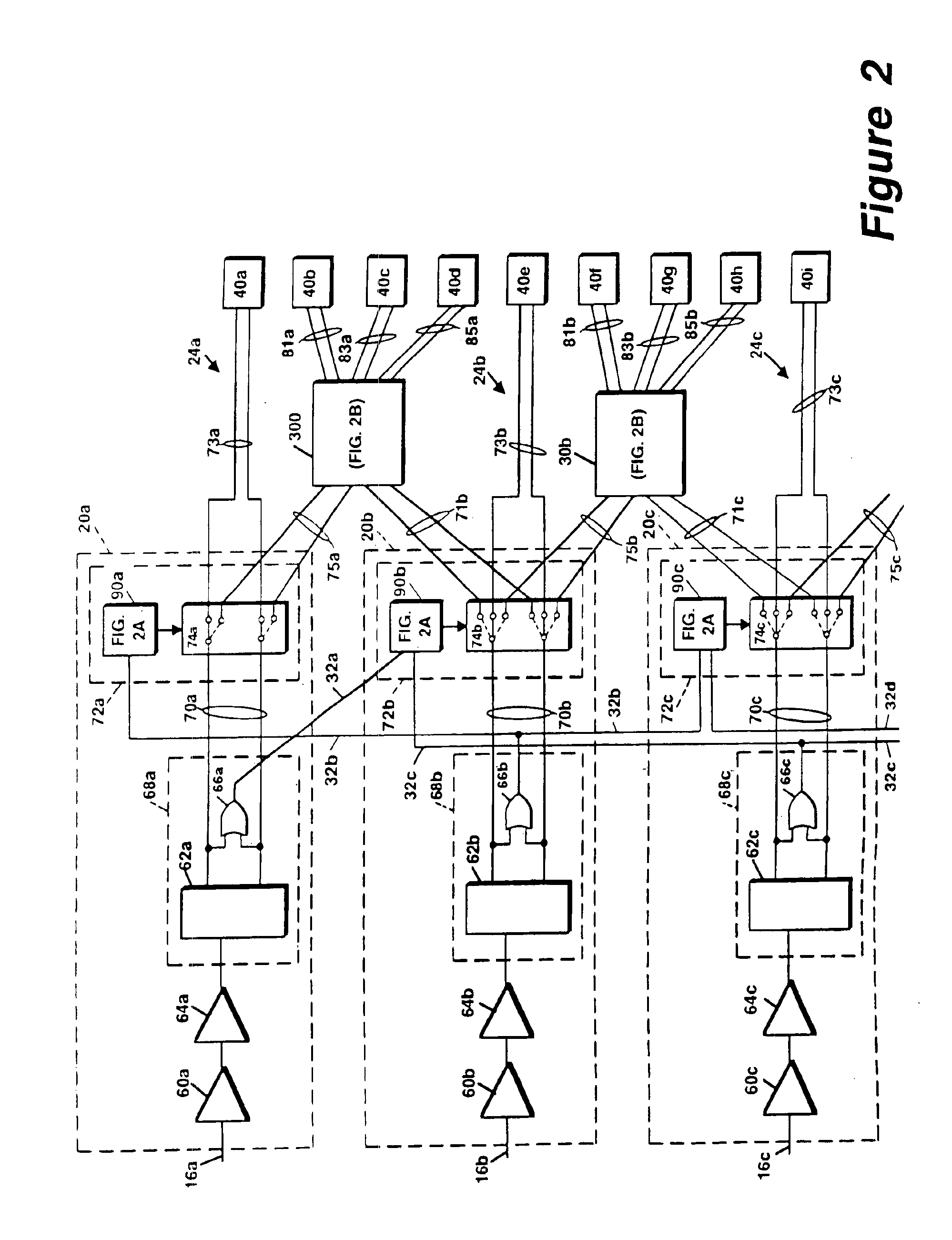
[0029]Referring to FIG. 1, an electronic imaging system 10 includes an imaging array 12 containing a plurality of radiation sensitive detector elements 14a-14n, each representing an image pixel, and a plurality of processing circuits 20a-20n, each responsive to a signal 16a-16n from a respective detector element and to a signal present indicator 32 from at least one other processing circuit associated with an adjacent detector element. The image processing circuitry 50 can be partitioned into channels 24a-24n, each of which accepts an input from at least one detector element 14a-14n and includes a processing circuit 20a-20n for processing the respective input signal(s). Each processing circuit 20a-20n samples its input at a sampling interval short enough, or equivalently at a sampling rate high enough, that only one signal event is likely to occur on a channel during the sampling interval (i.e., that the probability of a plurality of such events occurring in a sampling interval is n...


PUM


Abstract

An electronic imager includes a detector array, a plurality of processing circuits, each responsive to an output signal from a respective detector element of the array and to a determination that signal coupling in general or charge sharing in particular occurred. The imager further includes a shared channel circuit coupled to at least two processing circuits for receiving an output signal from the processing circuits in response to a determination that signal coupling has occurred and for generating an output signal in response to the received signals. The shared channel circuit further directs the output signal to an image sub-pixel, wherein a plurality of sub-pixels are associated with each radiation sensitive element.

Description

STATEMENTS REGARDING FEDERALLY SPONSORED RESEARCH[0001]This invention was made with government support under Contract No. F19628-00-C-0002 awarded by the Air Force. The government has certain rights in the invention.CROSS-REFERENCE TO RELATED APPLICATIONS[0002]Not applicable.FIELD OF THE INVENTION[0003]This invention relates to an electronic imager and more particularly to electronic imaging apparatus and techniques for improving resolution and reducing the effects of signal coupling between channels.BACKGROUND OF THE INVENTION[0004]Modern imaging has its roots in the nineteenth century with the advent of film which is used today for diverse applications, including generating common photographs and radiographic medical images using x-rays. During the past ten to twenty years, electronic imaging has become common in many fields and has totally replaced film systems in some applications. The term “electronic imaging” as used herein includes electro-optical imaging in the infrared, vis...

Claims


Application Information

Patent Timeline
Patent Type & Authority Patents(United States)
IPC IPC(8): H04N5/32H04N5/217
CPCH04N5/32H04N5/357H04N5/341H04N25/40H04N25/60
Inventor BEUSCH, JOHN U.
Owner MASSACHUSETTS INST OF TECH
Why Eureka
Try Eureka