Solid state image sensors and microlens arrays

a technology of image sensors and microlens arrays, applied in the field of solid state image sensors, can solve the problems of loss of sensitivity, degraded performance, loss of sensitivity, known as “vignetting” and other problems, and achieve the effect of reducing vignetting and mitigating the aforesaid disadvantages

Inactive Publication Date: 2005-04-26
STMICROELECTRONICS LTD
View PDF13 Cites 24 Cited by
  • Summary
  • Abstract
  • Description
  • Claims
  • Application Information

AI Technical Summary

Benefits of technology

[0009]It is an object of the present invention to provide an improved image sensor having a microlens array which reduces vignetting while mitigating the aforesaid disadvantages of the prior art.

Problems solved by technology

Light impinging on the non-sensitive pixel area is not collected, resulting in a loss of sensitivity and degraded performance.
However, if the shift is so extreme that the focussing spot is shifted partly or wholly out of the sensitive pixel area 200, as shown in FIG. 4, the pixel will fail to detect some or all of the light, resulting in a loss of sensitivity known as “vignetting.” This is particularly problematic with CMOS type image sensors which include a greater number of metal layers than, for example, CCD devices.
As a result, there is a larger distance between the microlens and the sensor surface, and this increases the shift of the focussing spot.
One attempt to address this problem is to increase the exit pupil of the primary lens system, but this is expensive and not cost effective for CMOS sensors which are generally used in low-cost imaging systems.
Also, the relative microlens shifts required for adjacent pixels are so small that it is impractical to apply the necessary displacements to individual microlenses in the manner disclosed in U.S. Pat. No. 5,610,390.

Method used


Image

  • Solid state image sensors and microlens arrays
  • Solid state image sensors and microlens arrays
  • Solid state image sensors and microlens arrays

Examples


Embodiment Construction

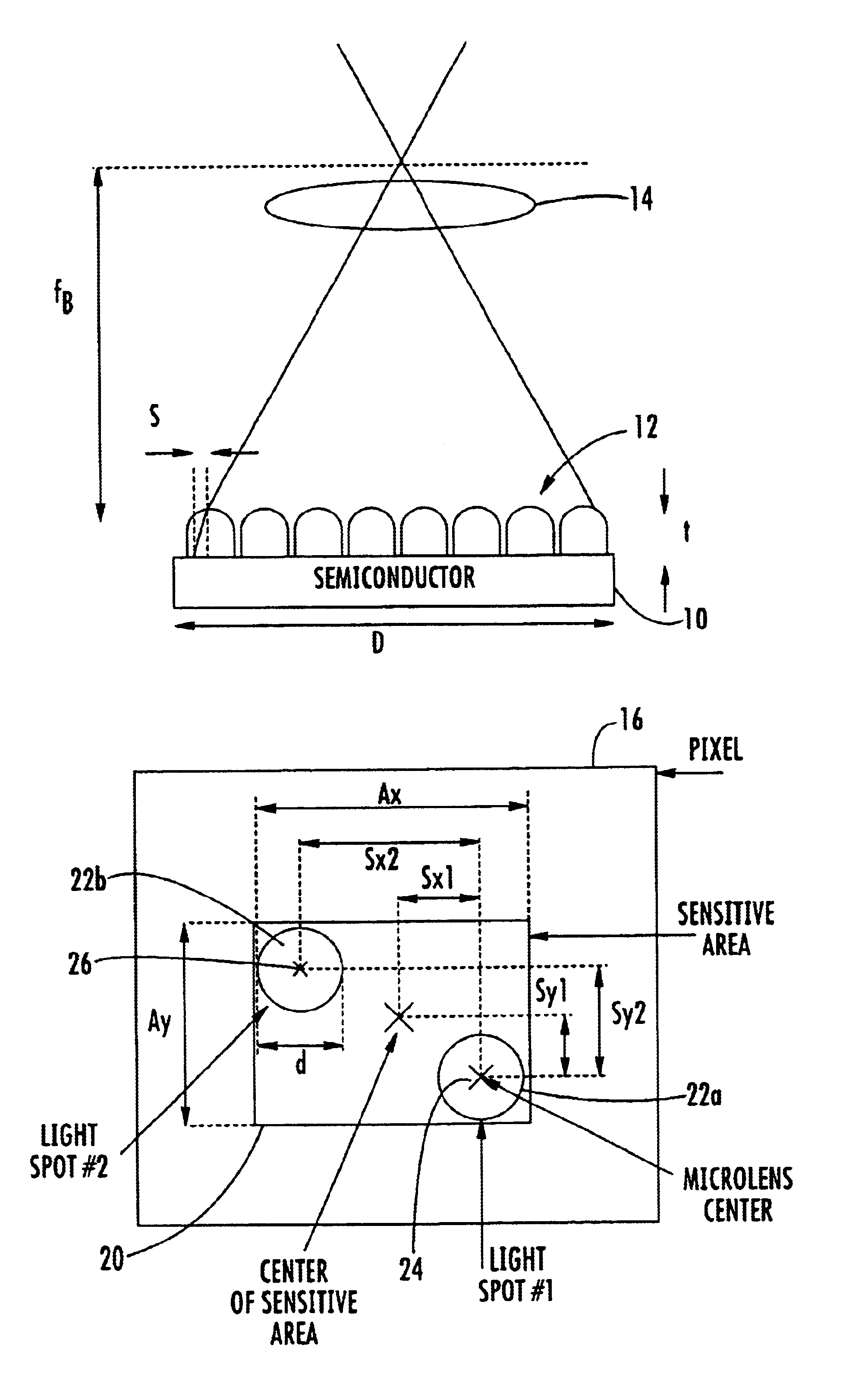
[0028]Referring now to FIG. 6, an imaging system according to the present invention includes a solid state image sensor 10 having a length / width D, a microlens array 12 having a thickness t and a refractive index n, and primary lens system 14 having a focal length fB. For a pixel at the edge of the sensor 10, the focussing spot is shifted away from the center of the sensor as a result of off-axis illumination by an amount s, where:

s=D×t / (2×fb×n).  (1)

The corresponding microlens would have to be shifted by the same amount in the opposite direction to compensate for this. Equation (1) is simplified for a one-dimensional (linear) sensor array, but is easily extended to two dimensions for a rectangular sensor array.

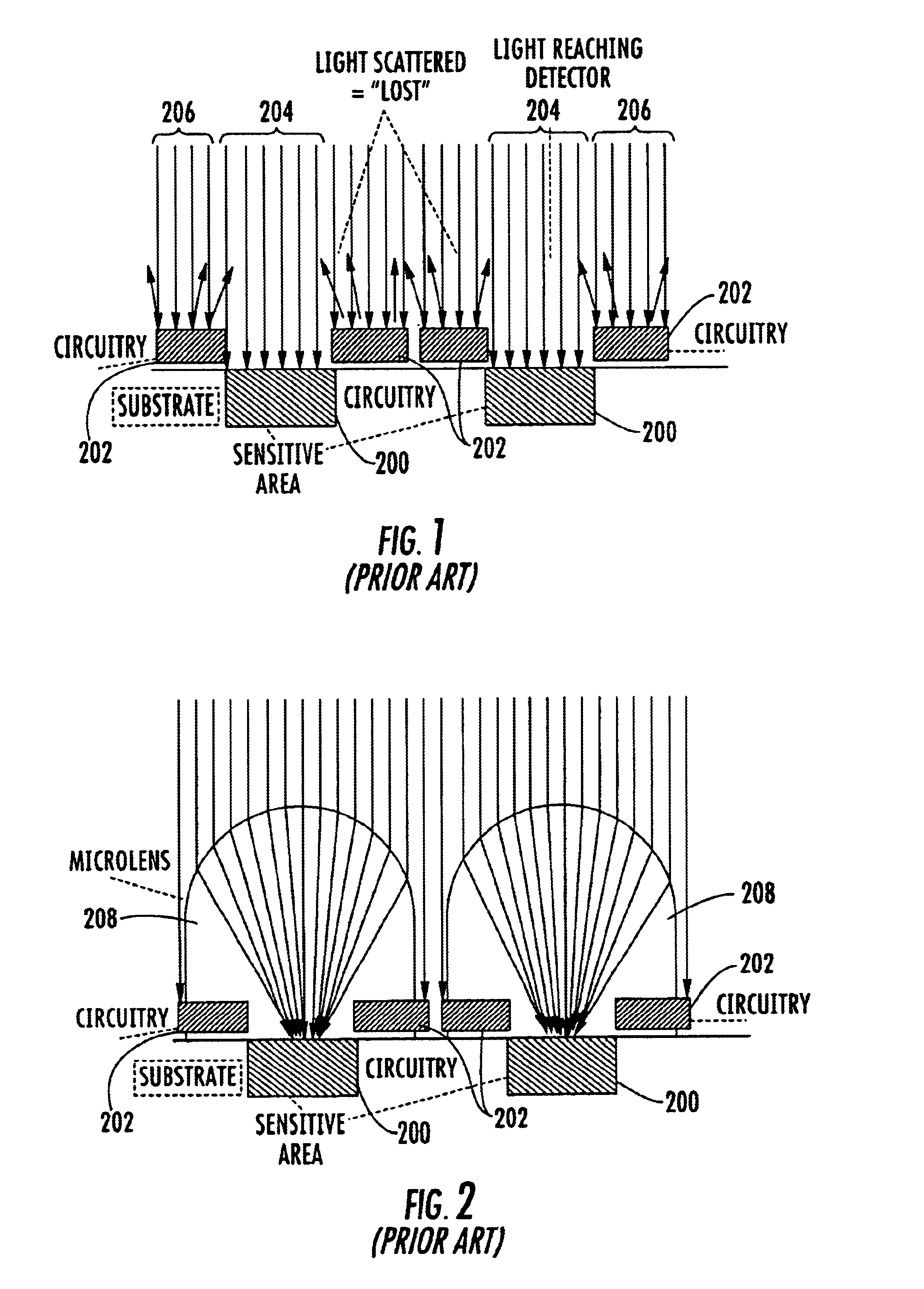
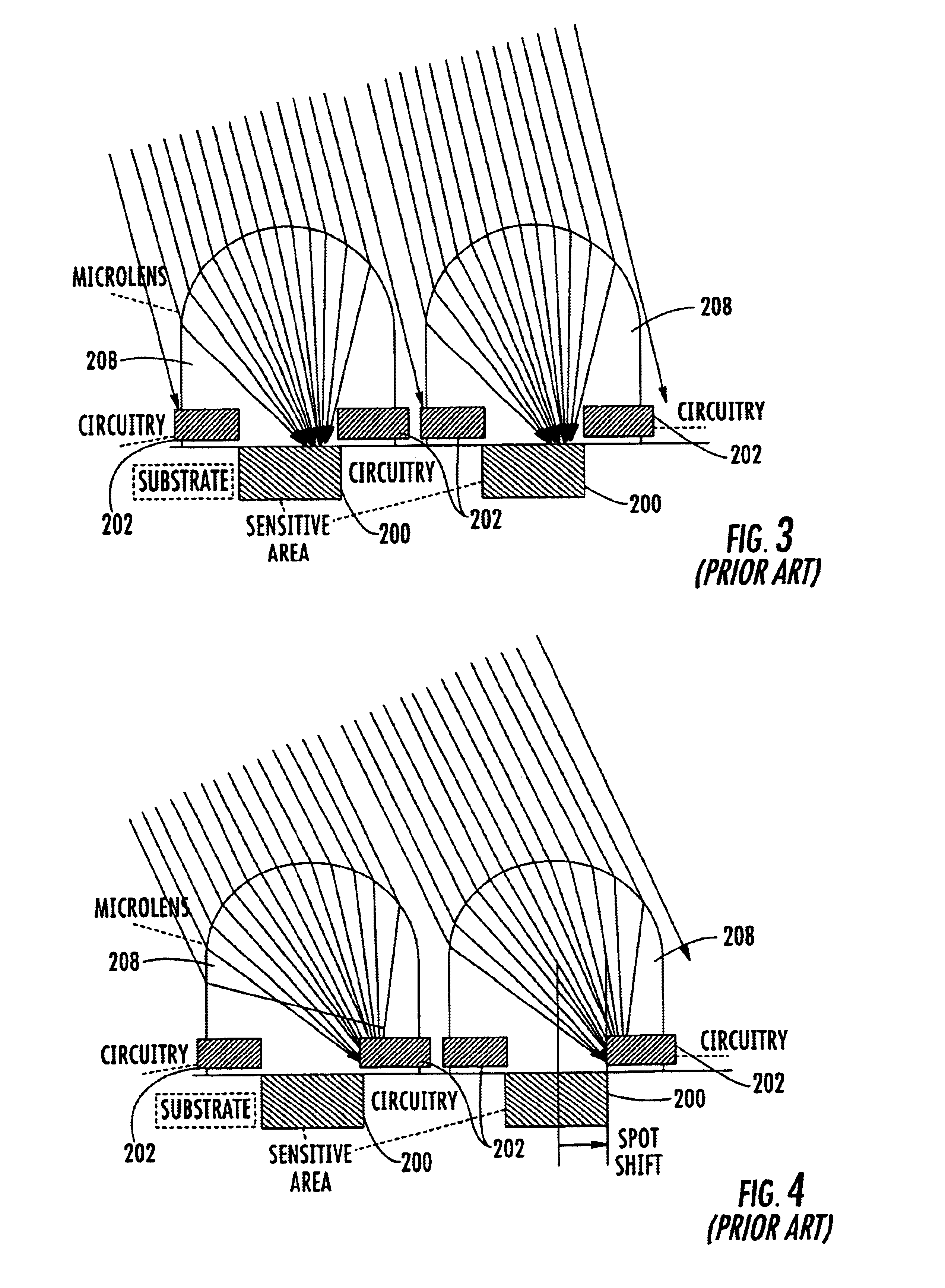
[0029]It will be understood that the present analysis is applicable to a range of types of primary lens systems including single- and multi-element lenses. Turning now to FIG. 7, the corresponding situation for a pixel 16 and microlens 18 located at the top left hand corner o...


PUM


Abstract

A solid state image sensor includes an array of pixels and a corresponding array of microlenses. The positions of the microlenses relative to their corresponding pixels may vary according to the distances of the pixels from a central optical axis of the image sensor to substantially eliminate vignetting of light collected by the microlenses.

Description

FIELD OF THE INVENTION[0001]The present invention relates to solid state image sensors of the type including an array of light sensitive elements (i.e., pixels) and, more particularly, to solid state image sensors including an array of microlenses disposed in front of the pixel array.BACKGROUND OF THE INVENTION[0002]A conventional solid state image sensor includes an array of light sensitive pixels. Not all of the area of each pixel is light sensitive. In a complementary metal-oxide semiconductor (CMOS) type image sensor, typically about 50% of the area of each pixel is occupied by opaque, non-sensitive circuitry. Light impinging on the non-sensitive pixel area is not collected, resulting in a loss of sensitivity and degraded performance. This is illustrated schematically in FIG. 1, which shows two adjacent pixels of a sensor array each including a sensitive area 200 surrounded by non-sensitive circuitry 202. Light 204 which strikes the sensitive areas 200 contributes to the sensor ...

Claims


Application Information

Patent Timeline
Patent Type & Authority Patents(United States)
IPC IPC(8): H01L27/146H01L29/04H01L29/02H01L31/18H01L31/0216H01L31/036H01L27/00H01L31/0376H01L31/20
CPCH01L27/14627
Inventor RAYNOR, JEFF
Owner STMICROELECTRONICS LTD
Why Eureka
Try Eureka