Thinned imaging lens group

An imaging lens and lens group technology, applied in optical components, optics, instruments, etc., can solve the problems of difficult to achieve miniaturization, limited refractive power, etc., and achieve the effect of shortening the total length, good imaging quality, and reducing the sensitivity of the system

Active Publication Date: 2011-11-09
LARGAN PRECISION
View PDF3 Cites 5 Cited by
  • Summary
  • Abstract
  • Description
  • Claims
  • Application Information

AI Technical Summary

Problems solved by technology

In order to correct aberrations, the form of a front aperture is generally used. For example, U.S. Patent No. 7,525,741 provides a thin imaging lens group composed of two lenses, bu

Method used


Image

  • Thinned imaging lens group
  • Thinned imaging lens group
  • Thinned imaging lens group

Examples


Example

[0073] "First Embodiment"

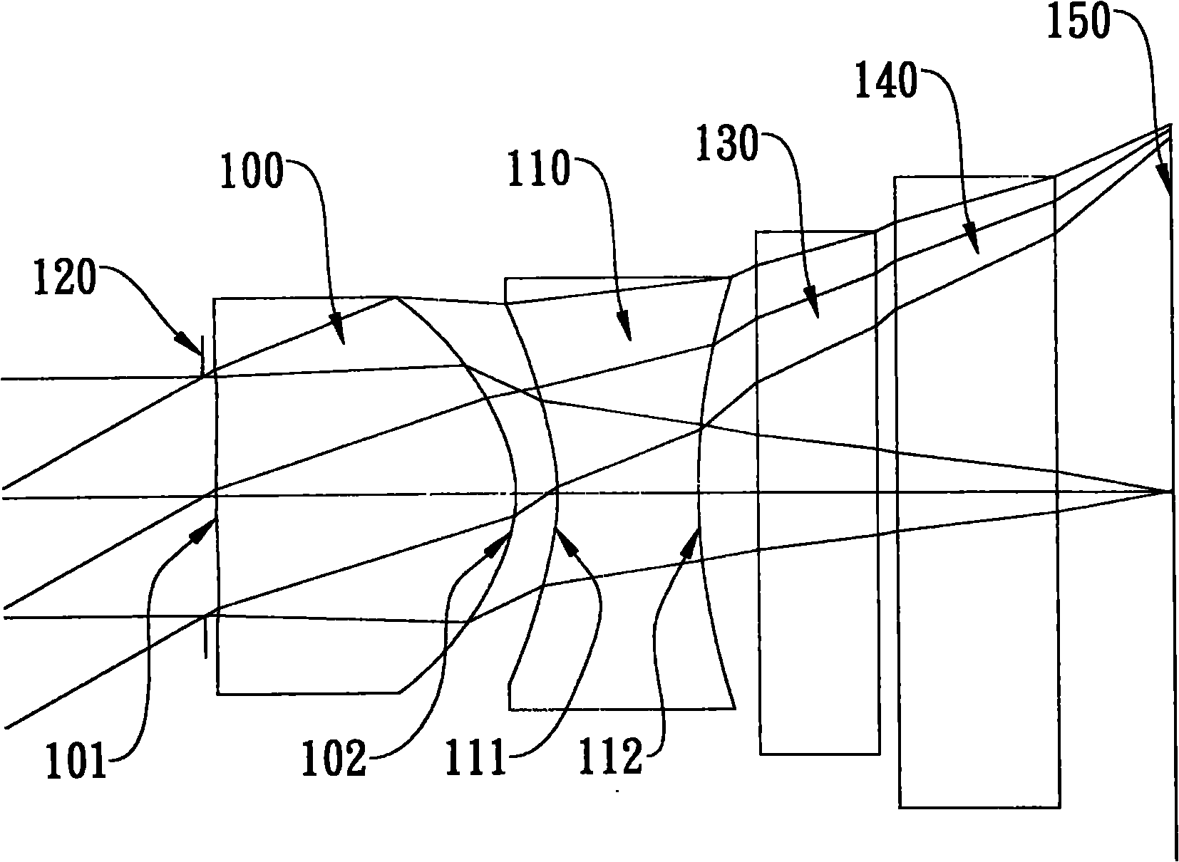
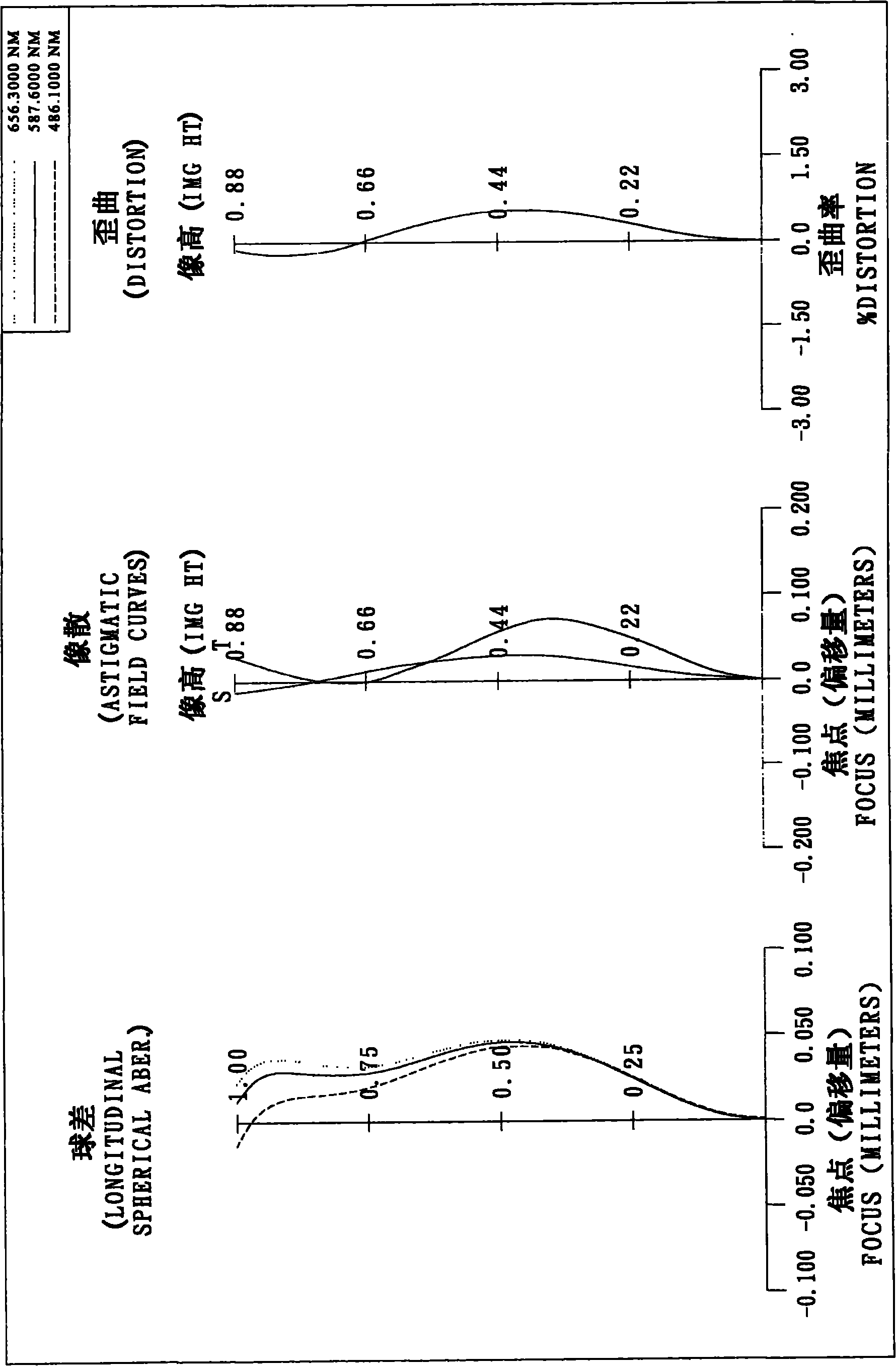
[0074] Please refer to the first embodiment of the present invention Figure 1A , please refer to the aberration curve of the first embodiment Figure 1B . The thin imaging lens group of the first embodiment is mainly composed of two lenses, which in sequence from the object side to the image side include:

[0075]A first lens (100) with positive refractive power, the object-side surface (101) of which is convex and the image-side surface (102) is convex, the material of which is plastic, and the object-side surface (101) of the first lens (100) ) and the image-side surface (102) are both aspherical; and

[0076] A second lens (110) with negative refractive power, the object-side surface (111) of which is concave and the image-side surface (112) is concave, the material of which is plastic, and the object-side surface (111) of the second lens (110) ) and the image side surface (112) are both aspherical;

[0077] Wherein, the thin imaging lens gr...

Example

[0102] "Second Embodiment"

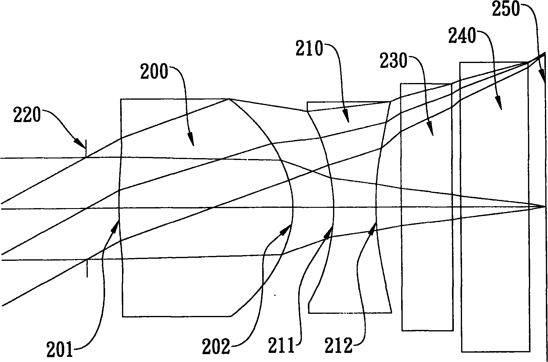
[0103] Please refer to the second embodiment of the present invention Figure 2A , please refer to the aberration curve of the second embodiment Figure 2B . The thin imaging lens group of the second embodiment is mainly composed of two lenses, which in sequence from the object side to the image side include:

[0104] A first lens (200) with positive refractive power, the object-side surface (201) of which is convex and the image-side surface (202) is convex, the material of which is plastic, and the object-side surface (201) of the first lens (200) ) and the image-side surface (202) are both aspherical; and

[0105] A second lens (210) with negative refractive power, the object-side surface (211) of which is concave and the image-side surface (212) is concave, the material of which is plastic, and the object-side surface (211) of the second lens (210) ) and the image side surface (212) are both aspherical;

[0106] Wherein, the thin imaging l...

Example

[0125] "Third Embodiment"

[0126] Please refer to the third embodiment of the present invention Figure 3A , please refer to the aberration curve of the third embodiment Figure 3B . The thin imaging lens group of the third embodiment is mainly composed of two lenses, which in sequence from the object side to the image side include:

[0127] A first lens (300) with positive refractive power, the object-side surface (301) of which is convex and the image-side surface (302) is convex, the material of which is plastic, and the object-side surface (301) of the first lens (300) ) and the image-side surface (302) are both aspherical; and

[0128] A second lens (310) with negative refractive power, the object-side surface (311) of which is concave and the image-side surface (312) is concave, the material of which is plastic, the object-side surface (311) of the second lens (310) ) and the image side surface (312) are both aspherical;

[0129] Wherein, the thin imaging lens grou...


PUM


Abstract

The invention discloses a thinned imaging lens group. From an object side to an image side, the lens group sequentially comprises a first lens with positive refractive power and a second lens with negative refractive power, wherein the object side surface of the first lens is a convex surface, the image side surface of the first lens is a convex surface, and at least one surface of the object side surface and the image side surface of the first lens is an aspheric surface; and the object side surface of the second lens is a concave surface, the image side surface of the second lens is a concave surface, and at least one surface of the object side surface and the image side surface of the second lens is an aspheric surface. The thinned imaging lens group is also provided with an aperture and an electric photosensitive device for imaging a photographed object; the aperture is arranged between the photographed object and the second lens; the electric photosensitive device is arranged on an imaging surface; and two lenses with refractive power are arranged in the thinned imaging lens group.

Description

technical field [0001] The present invention relates to a thin imaging lens assembly; in particular, to a thin imaging lens assembly applied to light and thin electronic products. Background technique [0002] In recent years, with the vigorous development of imaging modules, the demand for thin photographic lenses has been increasing, and the photosensitive devices of general photographic lenses are nothing more than charge coupled devices (CCDs) or complementary metal oxide semiconductor devices. (Complementary Metal-Oxide Semiconductor Sensor, CMOS Sensor), and with the advancement of semiconductor process technology, the pixel size of photosensitive devices has been reduced, and today's electronic products are characterized by good functions and light, thin and short appearance. , The thin imaging lens group with good imaging quality has become the mainstream in the current market. [0003] In order to consider the correction of aberrations, the traditional thin imaging...

Claims


Application Information

Patent Timeline
IPC IPC(8): G02B13/00G02B13/18
Inventor 蔡宗翰
Owner LARGAN PRECISION
Why Eureka
Try Eureka