Fringing capacitor structure

a capacitor and structure technology, applied in the field of capacitors, can solve the problems of significant increase in the cost of the device, unfavorable parasitic capacitance formation, and both options have drawbacks

Inactive Publication Date: 2005-04-26
MARVELL INT LTD
View PDF37 Cites 12 Cited by
  • Summary
  • Abstract
  • Description
  • Claims
  • Application Information

AI Technical Summary

Problems solved by technology

In addition to the device capacitance which is formed between the electrodes, there is also an undesirable parasitic capacitance that is formed between the substrate 19 and adjacent electrode.
Both of these options have drawbacks.
Increasing the plate area causes a further undesirable increase in the parasitic

Method used


Image

  • Fringing capacitor structure
  • Fringing capacitor structure
  • Fringing capacitor structure

Examples


Embodiment Construction

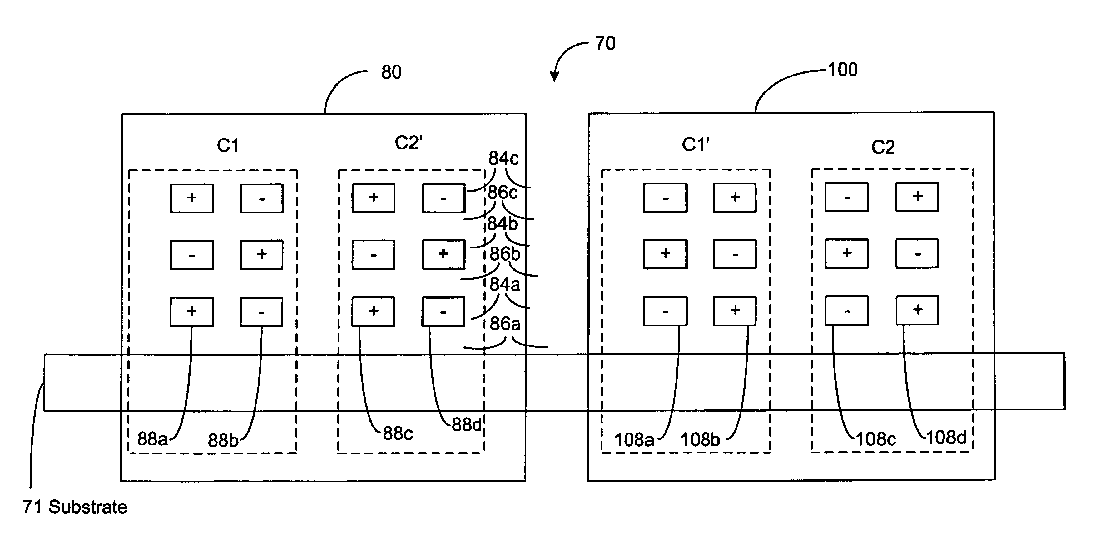
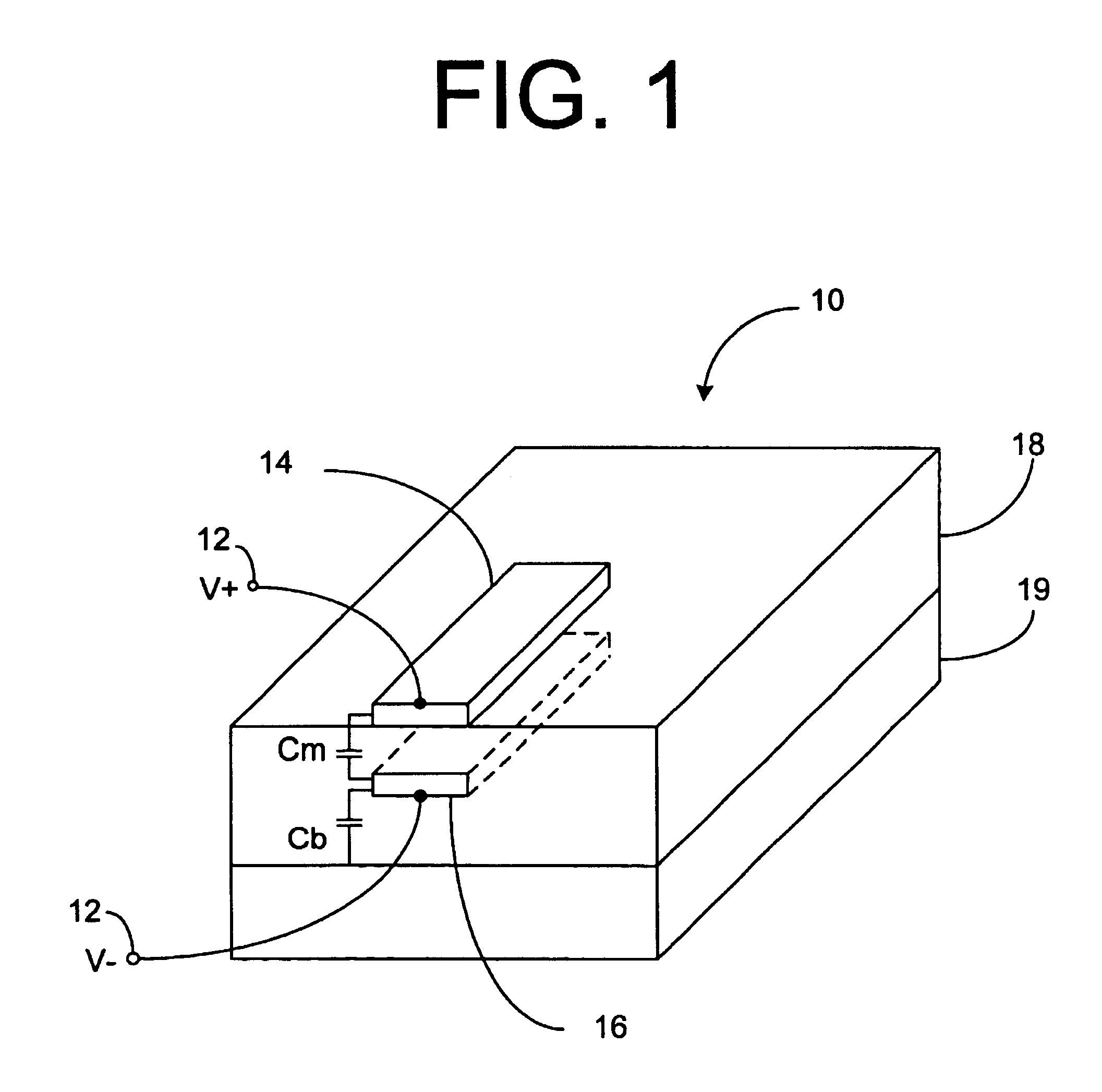
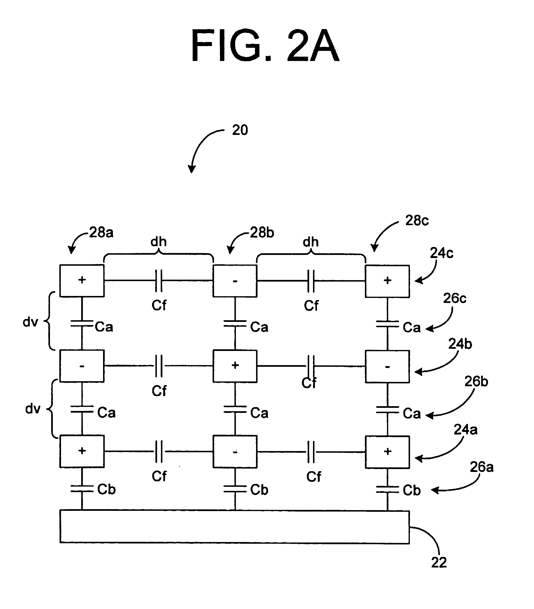
[0015]Referring to FIGS. 2A and 2B, illustrated are side and top views of a presently preferred embodiment of a fringing capacitor 20 fabricated on a semiconductor substrate 22 in accordance with the principles of the present invention. The fringing capacitor is particularly suitable for fabricating the device by using a conventional thin metal oxide process. The thin metal oxide process advantageously is less costly than complementary metal oxide semiconductor (CMOS) processes. However, using other semiconductor processes such as CMOS are also within the scope of the invention. The fringing capacitor 20 is particularly suitable for applications that require matched capacitors and high-density packaging.

[0016]The fringing capacitor 20 has a positive electrode 21 and a negative electrode 23. The positive and negative electrodes 21 and 23 are configured so that the device capacitance is formed between a combination of intralayer conductors as well as interlayer conductors. The fringin...


PUM


Abstract

The present invention provides a circuit and method for a fringing capacitor. The fringing capacitor includes at least two conductor layers spaced apart from each other. Each conductor layer includes at least two portions. The portions include odd ones alternating with even ones. Adjacent odd ones and even ones of the portions are spaced apart. The odd ones of the portions on a first one of the conductor layers are configured to substantially overlay the odd ones of the portions on an adjacent one of the conductor layers. The even ones of the portions on the first one of the conductor layers are configured to substantially overlay the even ones of the portions on the adjacent one of the conductor layers. The odd ones of the portions on the first one of the conductor layers are electrically coupled together and to the even ones of the portions on the adjacent one of the conductor layers, thereby defining a first electrode. The even ones of the portions on the first one of the conductor layers are electrically coupled together and to the odd ones of the portions on the adjacent one of the conductor layers, thereby defining a second electrode. A dielectric is interposed between the first and second electrodes. A guardband is spaced from the first and second electrodes.

Description

CROSS-REFERENCE TO RELATED APPLICATION[0001]This application is a continuation of U.S. patent application Ser. No. 09 / 765,200 filed on Jan. 18, 2001 now U.S. Pat. No. 6,625,006 which claims the benefit of U.S. Provisional Application No. 60 / 229,533, filed on Sep. 5, 2000, both of which are incorporated by referenced in their entirety.BACKGROUND OF THE INVENTION[0002]1. Field of the Invention[0003]The present invention relates generally to capacitors, and in particular to capacitors that are implemented within a semiconductor device.[0004]2. Discussion of the Related Art[0005]Conventional capacitors that are fabricated on semiconductor devices for storing charge are typically configured as metal-to-metal capacitors (MOMs). Referring to FIG. 1, the construction of a typical MOM 10 is illustrated. The MOM 10 includes two electrodes 12 that are formed on conductor layers 14 and 16 that are separated by a dielectric 18. A substrate 19 forms a base for the MOM 10. In addition to the devic...

Claims


Application Information

Patent Timeline
IPC IPC(8): H01G4/20H01G4/018H01L23/522H01L27/08
CPCH01L23/5223H01L27/0805H01L2924/3011H01L2924/0002H01L2924/00
Inventor ARAM, FARBODSUTARDJA, SEHAT
Owner MARVELL INT LTD
Why Eureka
Try Eureka