Method for making an integrated circuit package having reduced bow

a technology of integrated circuits and mounting packages, which is applied in the direction of semiconductor devices, semiconductor/solid-state device details, electrical apparatus, etc., can solve the problems of package to package, increase the bowing effect, and the molding compound is on either side of the parting line, so as to reduce the bow, reduce the cost, and reduce the effect of material consumption

Inactive Publication Date: 2005-05-03
MICRON TECH INC
View PDF12 Cites 4 Cited by
  • Summary
  • Abstract
  • Description
  • Claims
  • Application Information

AI Technical Summary

Benefits of technology

[0015]The integrated circuit package reduces bow when the parting line is offset from the center of a side surface. A further benefit is that the support is maintained on the perimeter of the package, and the package is sturdy enough to withstand the rigor of the trim and form machine. A cost savings is enjoyed also since less material is used to make the package. In addition, the package is aesthetically pleasing to the customer.

Problems solved by technology

As the packaging is produced, often the parting line formed during the overmolding process is offset from the center of the packaging, resulting in an imbalance of the molding compound on either side of the parting line.
As the molding compound is cured, the imbalance of compound causes the package to bow.
As the geometries diminish, the imbalance of compound becomes greater, resulting in increasing bowing effect.
However, this was not effective in reducing bow and results in weaker components which can chip and crack during the trimming and forming of the leadframe.
In addition, this can result an increased chance of inadvertently exposing the semiconductor component to the environment.

Method used


Image

  • Method for making an integrated circuit package having reduced bow
  • Method for making an integrated circuit package having reduced bow
  • Method for making an integrated circuit package having reduced bow

Examples


Embodiment Construction

[0028]In the following detailed description, reference is made to the accompanying drawings which form a part hereof, and in which is shown by way of illustration specific embodiments in which the invention may be practiced. These embodiments are described in sufficient detail to enable those skilled in the art to practice the invention, and it is to be understood that other embodiments may be utilized and that structural changes may be made without departing from the scope of the present invention. Therefore, the following detailed description is not to be taken in a limiting sense, and the scope of the present invention is defined by the appended claims and their equivalents.

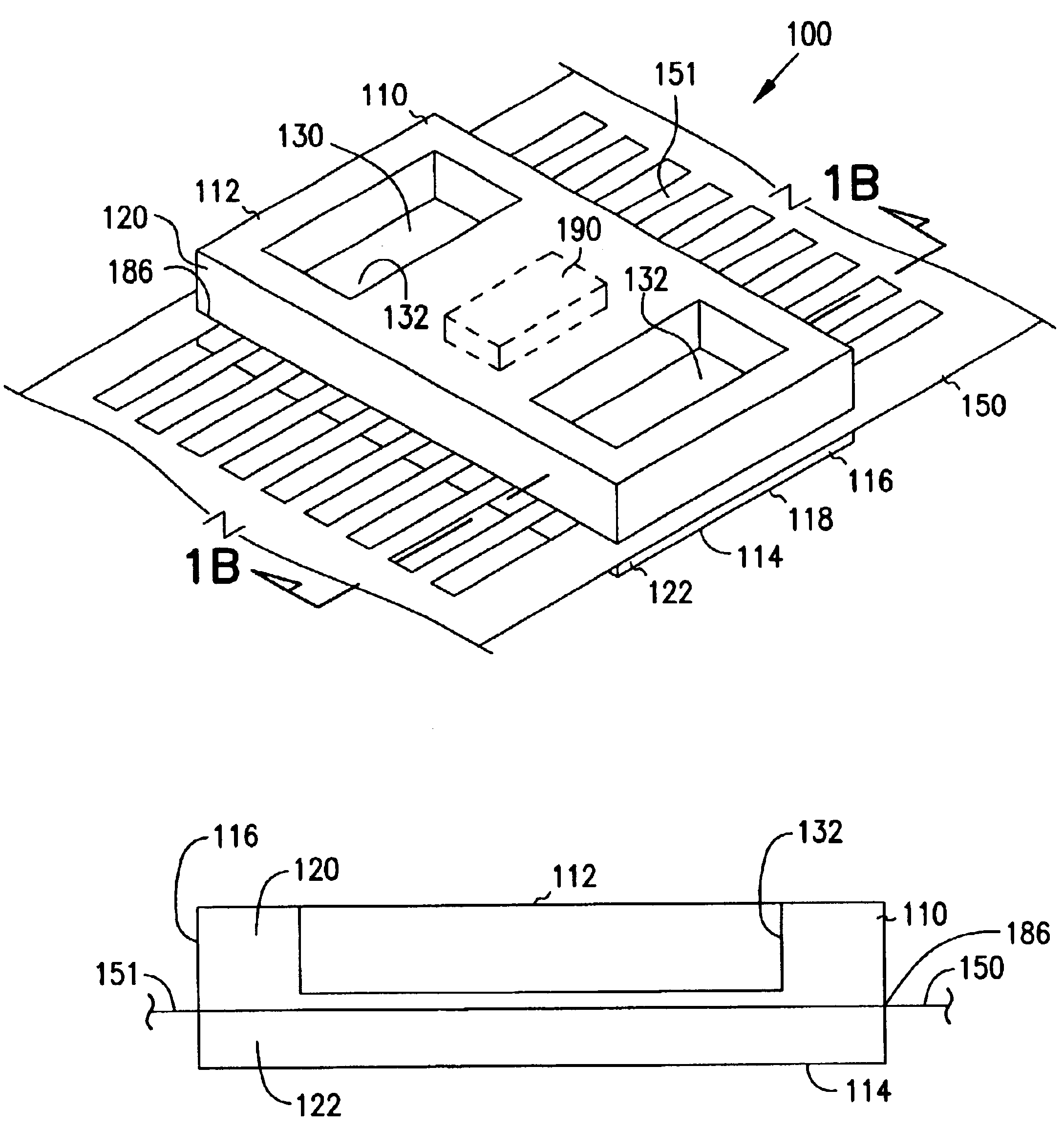
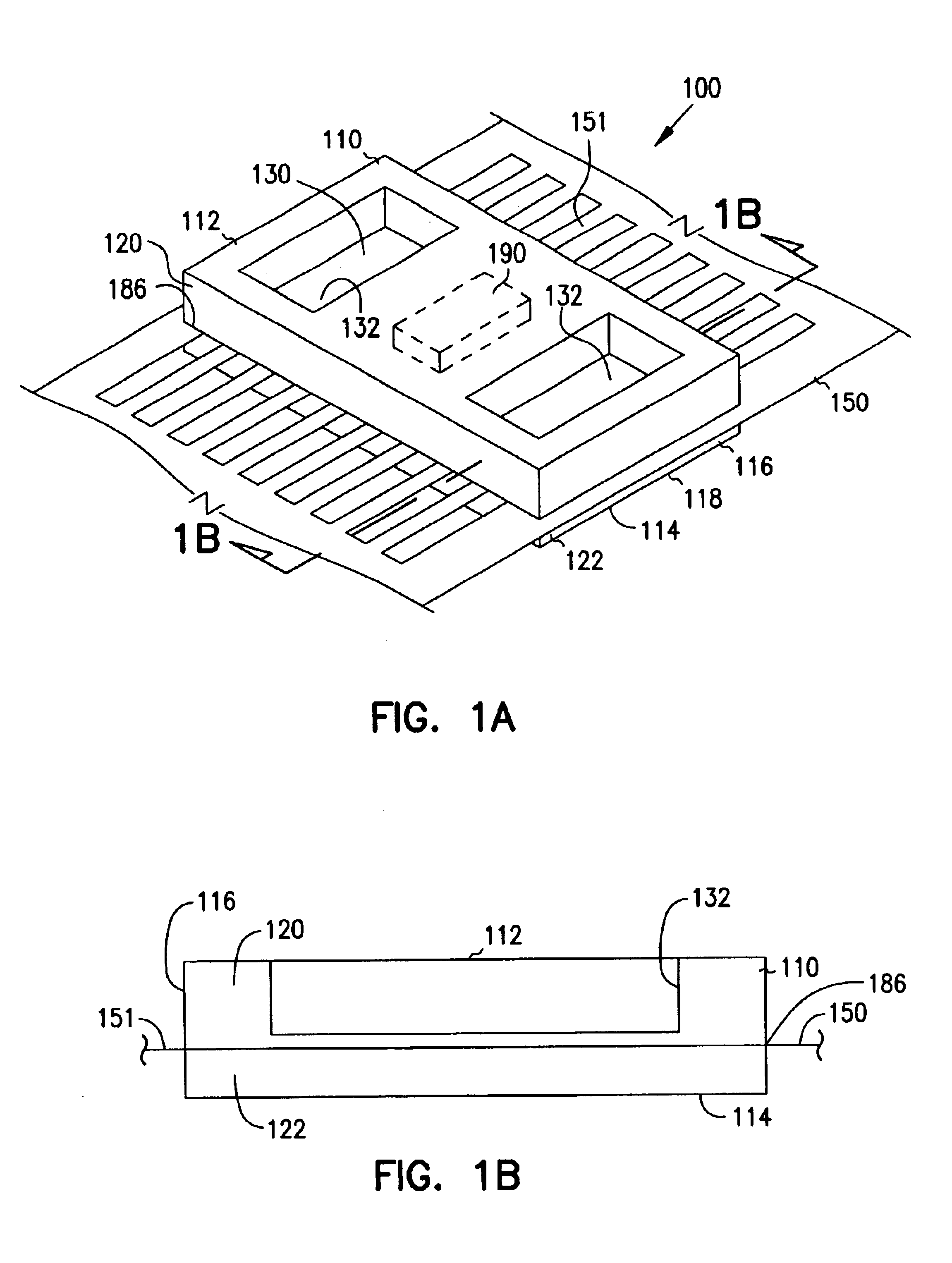
[0029]FIG. 1 illustrates a perspective view of an integrated circuit device 100 constructed in accordance with one embodiment. The integrated circuit device 100 generally includes an integrated circuit package 110, a lead frame 150 including at least one conductor 151, and at least one semiconductor component ...


PUM


Abstract

An integrated circuit device includes a semiconductor component coupled with a lead frame, and an integrated circuit package encompassing at least a portion of the semiconductor component. The package has a first surface and a second surface, and side surfaces, where the first surface is opposite the second surface. A parting line of the integrated circuit package is offset toward the second surface of the package, where the first surface optionally comprises the bottom surface of the package. The first surface of the package has one or more recessed areas.

Description

RELATED APPLICATION[0001]This application is a Divisional of U.S. application Ser. No. 09 / 648,316 filed on Aug. 25, 2000 now U.S. Pat. No. 6,577,018 which is incorporated herein by reference.FIELD OF THE INVENTION[0002]The present invention relates generally to semiconductor mounting packages. More particularly, it pertains to reducing bow for a semiconductor mounting package.BACKGROUND OF THE INVENTION[0003]Integrated circuits include packaging which houses sensitive semiconductor components. The semiconductor components, and their packaging, are being produced with diminishing geometries such that an electronic circuit board with increased density can be produced. As the packaging is produced, often the parting line formed during the overmolding process is offset from the center of the packaging, resulting in an imbalance of the molding compound on either side of the parting line. As the molding compound is cured, the imbalance of compound causes the package to bow. As the geometr...

Claims


Application Information

Patent Timeline
Patent Type & Authority Patents(United States)
IPC IPC(8): H01L23/28H01L23/31H01L23/498H01L23/48
CPCH01L23/3107H01L23/495H01L23/49805H01L23/562H01L2924/0002H01L2924/19041H01L2924/00
Inventor TANDY, WILLIAM D.SCHWAB, MATT E.BAERLOCHER, CARY J.
Owner MICRON TECH INC
Why Eureka
Try Eureka