Light emitting diode

a technology of light-emitting diodes and diodes, which is applied in the direction of semiconductor/solid-state device manufacturing, semiconductor devices, electrical apparatus, etc., can solve the problems of reducing reducing the footprint, and limiting the number of devices that can be constructed, so as to increase the light output efficiency of the device and increase the density of the devi

Inactive Publication Date: 2005-05-03
DALIAN MEIMING EPITAXIAL WAFER TECH
View PDF9 Cites 21 Cited by
  • Summary
  • Abstract
  • Description
  • Claims
  • Application Information

AI Technical Summary

Benefits of technology

[0004]A light emitting diode, in accordance with one embodiment consistent with the present invention, includes a complementary pair of electrodes and a mechanism for isolating their corresponding metal contacts, to force current ...

Problems solved by technology

Although the structures of light emitting diodes (LED's) and the manufacturing processes for making those structures have matured through the years, there remain technical and economic challenges to the industry.
A particular challenge to reduction of the footprint exists in the ...

Method used


Image

  • Light emitting diode
  • Light emitting diode

Examples


Embodiment Construction

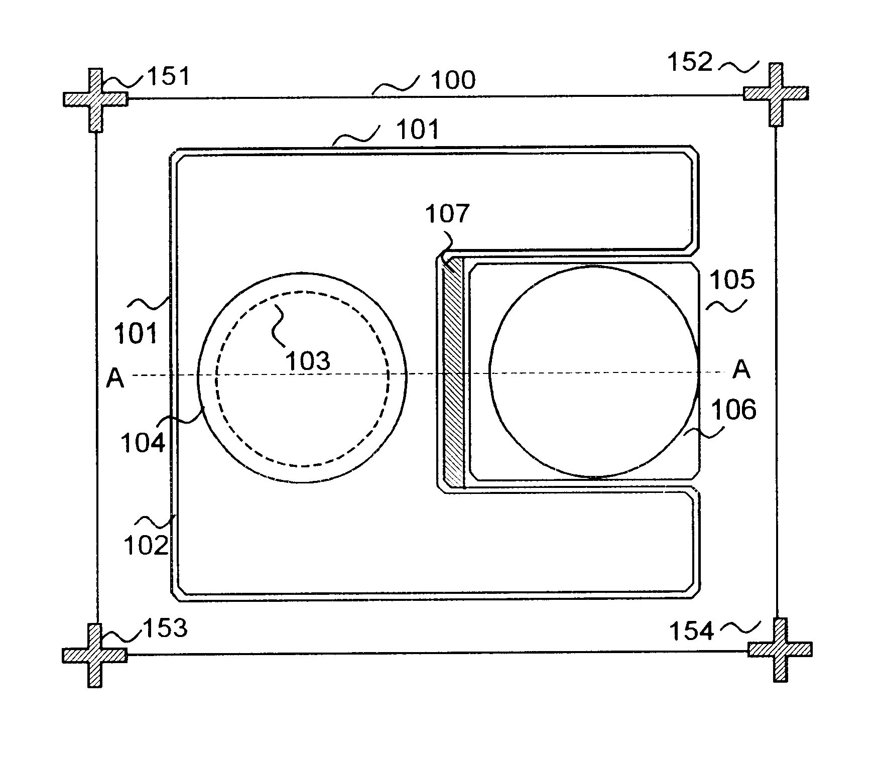
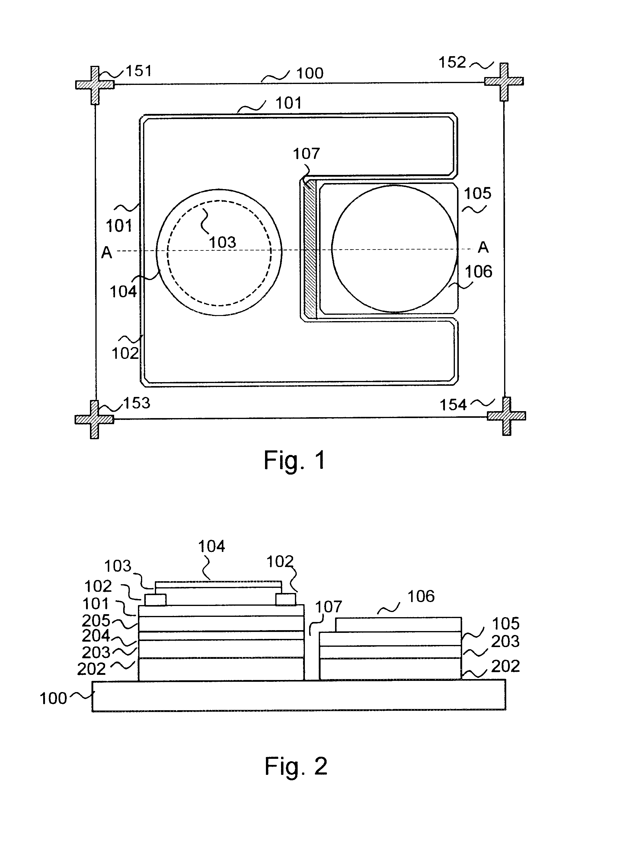
[0008]For purposes of illustration, an LED depicted in FIGS. 1 and 2 is a gallium nitride (GaN) based structure formed on an insulating substrate. The device of FIG. 1 is surrounded by four plus symbols, i.e., reference numerals 151 through 154, and by a boundary line of the substrate 100 to demonstrate an illustrative footprint of a device on the substrate. The devices of FIG. 1, as formed on substrate 100, are separated by “streets” which have been formed by etching. Separation of the devices is nominally along the center lines of the streets.

[0009]In FIGS. 1 and 2, the same reference numerals depict the same elements. The features of FIG. 2, which are not illustrated in FIG. 1, are identified with reference numerals starting at 202.

[0010]The illustrative GaN device consistent with one embodiment of the present invention, and as shown in FIGS. 1 and 2, is formed on a sapphire substrate 100. FIG. 2 illustrates the components of the LED as seen at the section line A—A of FIG. 1. The...


PUM


Abstract

A semi-conductor light emitting diode includes closely spaced n and p electrodes formed on the same side of a substrate to form an LED with a small foot-print. A semi-transparent U shaped p contact layer is formed along three sides of the top surface of the underlying window layer. The p electrode is formed on the p contact layer centered on the closed end of the U shaped layer. An n contact layer is formed on an n cladding layer and centered in the open end of the U of the p contact layer. The n electrode is formed on the n contact layer. The n and p electrodes are electrically isolated from one another by either a trench or an insulator, situated between the electrodes.

Description

[0001]The present invention relates to light emitting diodes which have metal contacts on the same side of a substrate.BACKGROUND OF THE INVENTION[0002]Although the structures of light emitting diodes (LED's) and the manufacturing processes for making those structures have matured through the years, there remain technical and economic challenges to the industry. Because of the high costs of substrates and growth processes, it is essential to the success of the manufacturing processes, that the footprint of each device be kept as small as possible that is consistent with the target light output requirements.[0003]A particular challenge to reduction of the footprint exists in the case of LED's which employ insulating substrates and metal contacts which are situated on the same side of the substrate. In such structures, there is a tendency for current flowing between the metal contacts to concentrate in a small, lower impedance, preferred path through the light emitting surface. Conseq...

Claims


Application Information

Patent Timeline
IPC IPC(8): H01L33/00H01L33/14H01L33/20H01L33/32H01L33/38
CPCH01L33/145H01L33/38H01L33/20H01L33/32
Inventor LIU, HENGCHEN, CHANGHUA
Owner DALIAN MEIMING EPITAXIAL WAFER TECH
Why Eureka
Try Eureka