Semiconductor chip and structure for mounting same

A mounting structure and semiconductor technology, applied in semiconductor devices, semiconductor/solid-state device manufacturing, electric solid-state devices, etc., can solve the problem that conductive particles are difficult to be captured between electrodes, and achieve the effect of suppressing insufficient flow

Inactive Publication Date: 2012-05-16
SHARP KK
View PDF6 Cites 11 Cited by
  • Summary
  • Abstract
  • Description
  • Claims
  • Application Information

AI Technical Summary

Problems solved by technology

Therefore, ACP has the disadvantage that conductive particles are difficult to be captured between electrodes during bonding.

Method used


Image

  • Semiconductor chip and structure for mounting same
  • Semiconductor chip and structure for mounting same
  • Semiconductor chip and structure for mounting same

Examples


no. 1 approach

[0093]

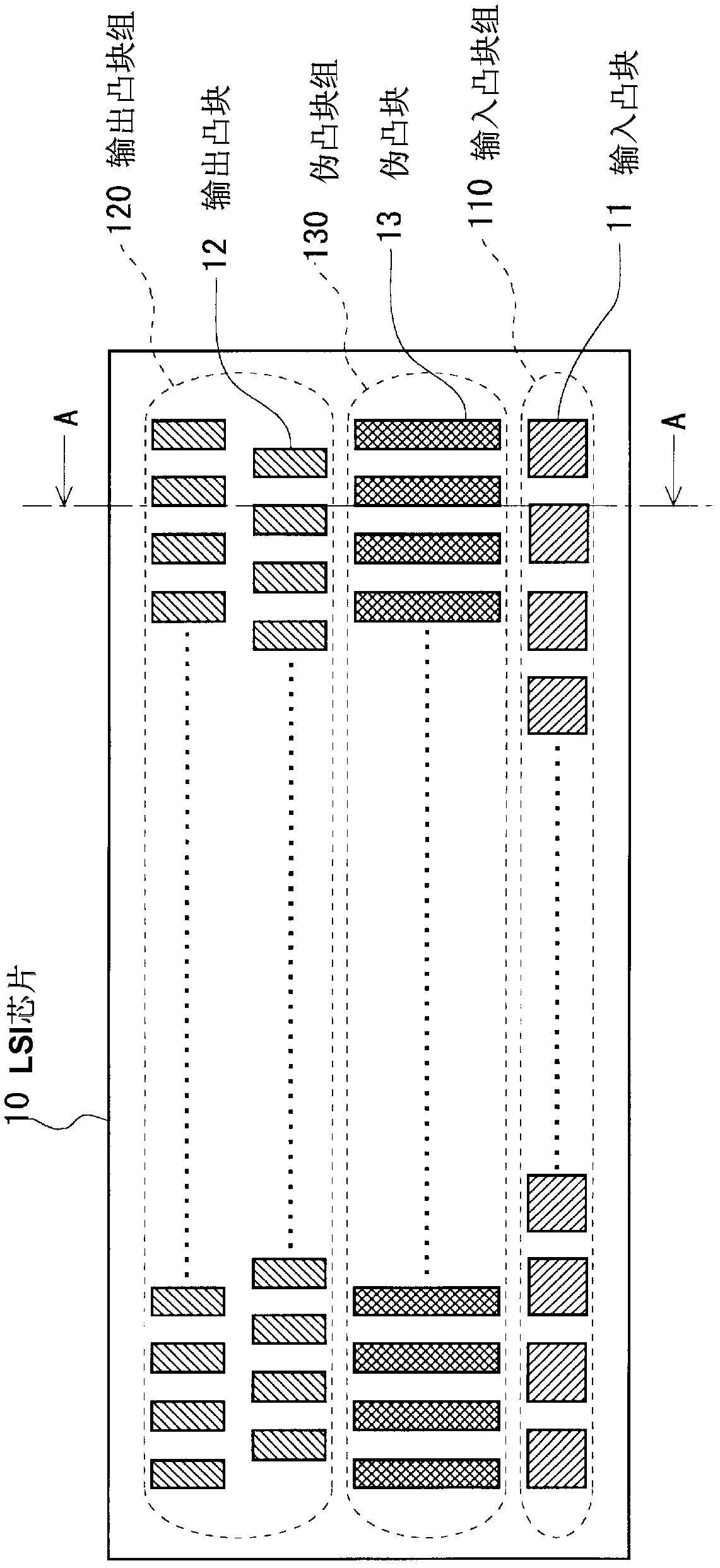
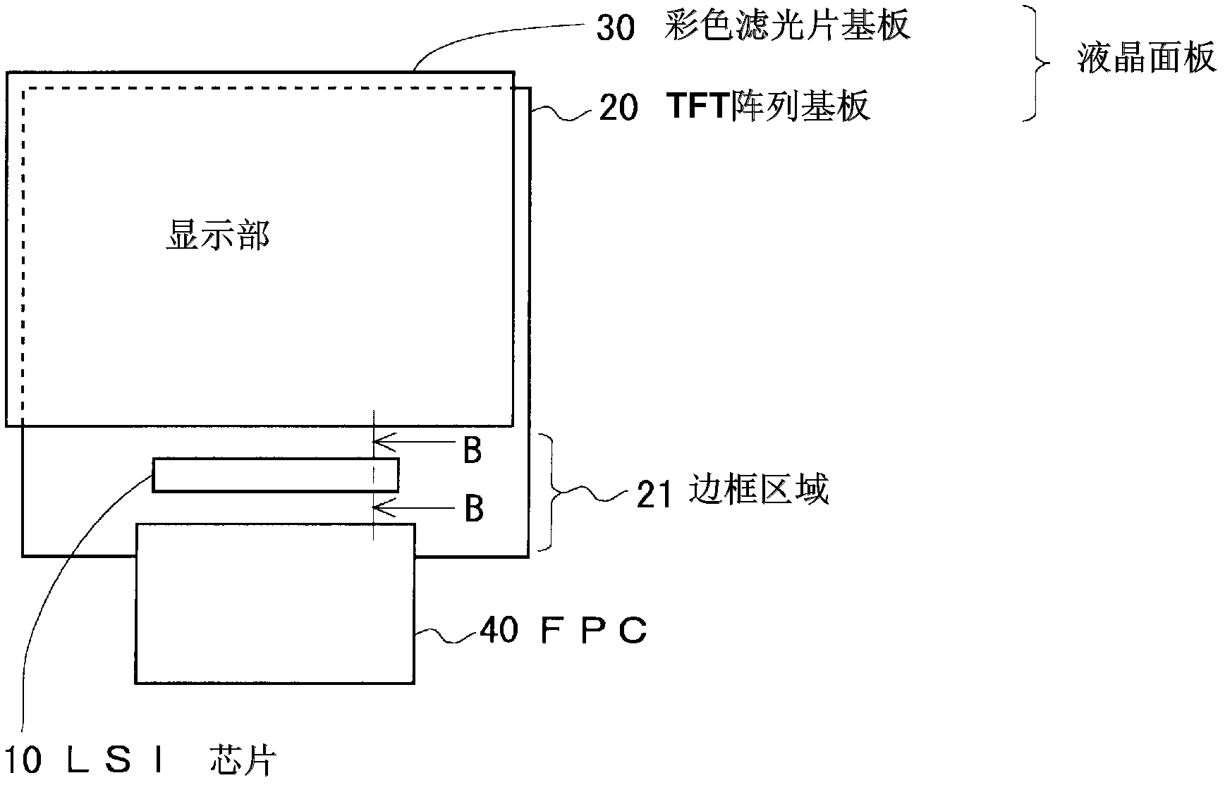
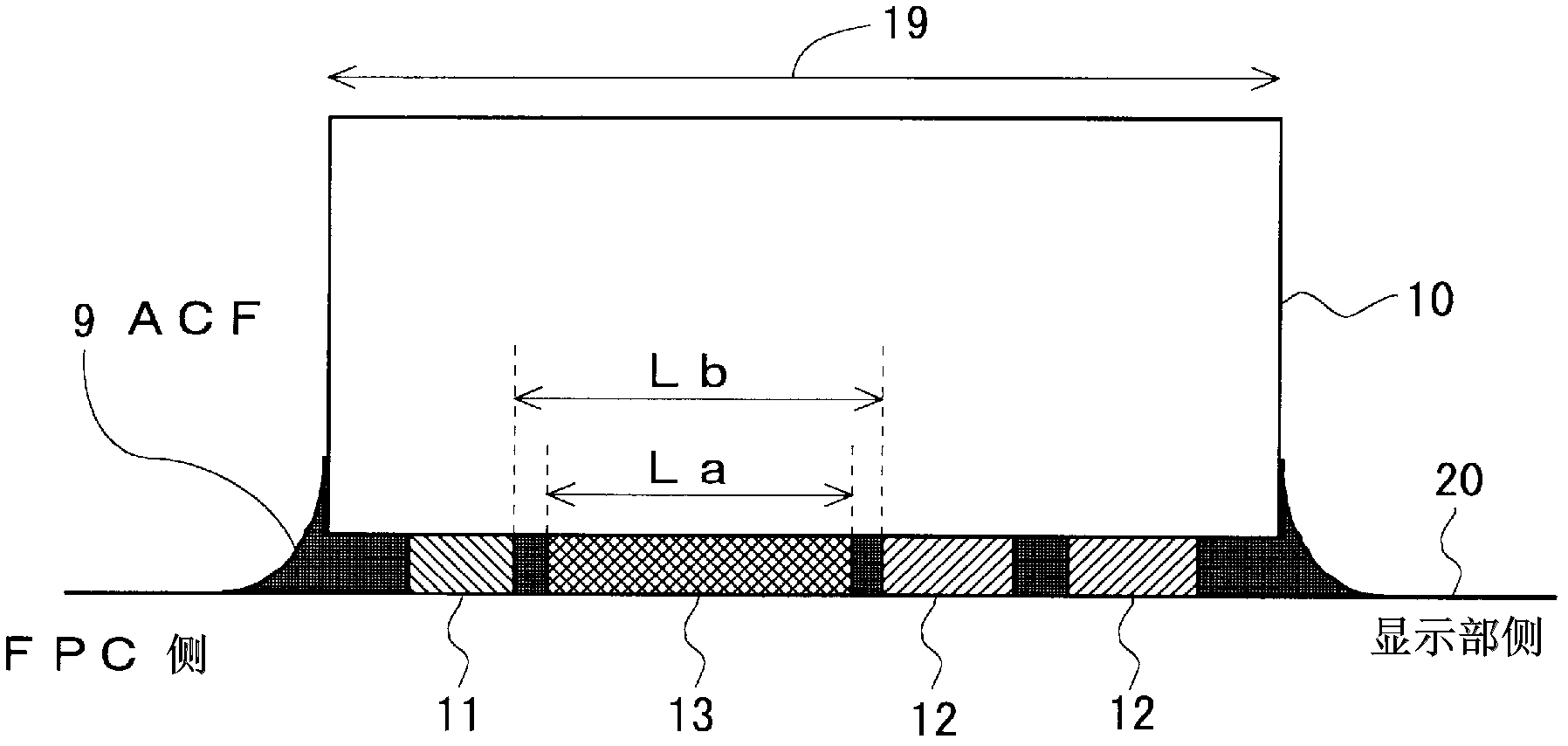
[0094] figure 2 It is a plan view of a liquid crystal module including an LSI chip (semiconductor chip) according to the first embodiment of the present invention. This liquid crystal module includes a liquid crystal panel, an LSI chip 10 and an FPC (Flexible Printed Circuit: flexible printed circuit) 40 . The liquid crystal panel includes: a TFT array substrate 20 that includes pixel electrodes (display electrodes) and is formed with a TFT array; The color filter substrate 30 of the opposite electrode. Both the TFT array substrate 20 and the color filter substrate 30 are glass substrates. Additionally, if figure 2 As shown, the TFT array substrate 20 is larger in plan view than the color filter substrate 30 . A display unit is provided in a region where the TFT array substrate 20 and the color filter substrate 30 overlap in a plan view. The area on the TFT array substrate 20 that is not opposite to the color filter substrate 30 is generally called a "frame"....

no. 2 approach

[0106] Figure 7 It is a bottom view of the LSI chip 10 according to the second embodiment of the present invention. In this embodiment, if Figure 7 As shown, the dummy bumps 13 are provided only near one short side and the other short side of the bottom surface of the LSI chip 10 . That is, the plurality of bumps 13 included in the bump group 130 of the first embodiment described above (refer to figure 1 ) are formed on the bottom surface of the LSI chip 10 on the outermost two bumps 13 . The configuration other than that is the same as that of the above-mentioned first embodiment, so description thereof will be omitted.

[0107] The more dummy bumps 13 that suppress the flow of the ACF resin from the central portion to the short sides are provided in the area between the input bump group 110 and the output bump group 120, the more reliable the connection between the LSI chip 10 and the TFT array substrate 20 will be. The higher the sex. However, the greater the number...

no. 3 approach

[0109] Figure 8It is a bottom view of the LSI chip 10 according to the third embodiment of the present invention. Various restrictions can be imposed on the formation of the bumps on the bottom surface of the LSI chip 10 . For example, the length of the long side of the bump may be limited to a predetermined length or less. In such a case, the distance between the input bump group 110 and the dummy bump group 130 or the distance between the output bump group 120 and the dummy bump group 130 becomes large, and it can be considered that the ACF resin moves from the center to the short side. The large flow on the side is not hindered. Therefore, in this embodiment, if Figure 8 As shown, the dummy bump group 130 is formed as follows: the dummy bumps 13 arranged on one long side of the bottom surface of the LSI chip 10 and the dummy bumps 13 arranged on the other long side of the bottom surface of the LSI chip 10 alternately. configuration. The configuration other than that ...


PUM


Abstract

Provided is a semiconductor chip which can suppress generation of failures of connection with a substrate having the semiconductor chip mounted thereon and has a narrow pitch between the terminals. The LSI chip (10) includes an input bump group (110), which is composed of a plurality of input bumps (11) disposed in a row along one of the long sides of the bottom surface, and an output bump group (120), which is composed of a plurality of output bumps (12) disposed in zigzag arrangement along the other long side of the bottom surface. In the LSI chip, a dummy bump group (130) composed of a plurality of rectangular dummy bumps (bumps not having an electrically connecting function) (13), each of which has, as the long sides, the sides extending in the direction perpendicular to the long sides of the bottom surface is provided in the region between the region provided with the input bump group (110) and the region provided with the output bump group (120).

Description

technical field [0001] The present invention relates to a semiconductor chip and its mounting structure, and more specifically, to a structure of a semiconductor chip mounted on a substrate with a conductive adhesive, and a mounting structure obtained by mounting such a semiconductor chip on a substrate. Background technique [0002] In recent years, there has been an increasing demand for miniaturization and thinning of electronic equipment. Along with this, there are various methods of mounting IC (Integrated Circuit: Integrated Circuit) chips and LSI (Large Scale Integration: Large Scale Integrated Circuits) chips (hereinafter both will be combined and simply referred to as "chips") on wiring boards. proposal. For example, a mounting method called "flip chip mounting" is known as a method of mounting a chip on a wiring board in an extremely small area. The so-called flip-chip method is to form protruding electrodes called "bumps" on the surface of an unpackaged chip cal...

Claims


Application Information

Patent Timeline
Patent Type & Authority Applications(China)
IPC IPC(8): H01L21/60
CPCH01L24/83H01L2924/0781H01L24/29H01L2224/2929H01L2924/00014H01L2224/83101H01L24/92H01L2224/13013H01L2224/14177G02F1/1333H01L2924/00013H01L2224/13099H01L2224/16225H01L2924/01004H01L2224/1403H01L2924/01078H01L2924/01006H01L2224/14136H01L2224/0603H01L2224/29298H01L2924/01079H01L2924/14H01L2224/83203H01L2224/26145H01L24/73H01L2224/83192H01L2924/01005H01L2224/29299H01L2924/01057H01L2224/73204H01L2224/2919H01L2224/83851H01L2224/81193H01L2224/0401H01L2224/14517H01L2224/14152H01L24/32H01L2224/14153H01L2924/01033H01L24/14H01L2924/0665H01L24/81H01L2224/14131H01L2224/14133H01L2224/14151H01L2224/14155H01L2224/14156H01L21/563H01L24/13H01L24/16H01L2224/32225H01L2224/81191H01L2224/9211H01L2924/381H01L2224/14135H01L2224/81903H01L2924/15788H01L2224/17517H01L2924/00H01L2224/29099H01L2224/29199H01L2224/81H01L2224/83
Inventor 盐田素二中滨裕喜松井隆司堀口武志
Owner SHARP KK
Why Eureka
Try Eureka