Organic semiconductor devices and methods of fabrication

a technology of organic semiconductors and semiconductor devices, applied in semiconductor devices, solid-state devices, thermoelectric devices, etc., can solve the problems of inability to achieve inorganic semiconductor-based devices, the efficiency and operation stability of hetrojunction systems are still far below what has been achieved with inorganic semiconductor-based devices, and the complexity of fullerence derivative fabrication

Inactive Publication Date: 2005-05-10
XIAO STEVEN SHUYONG
View PDF2 Cites 49 Cited by
  • Summary
  • Abstract
  • Description
  • Claims
  • Application Information

AI Technical Summary

Problems solved by technology

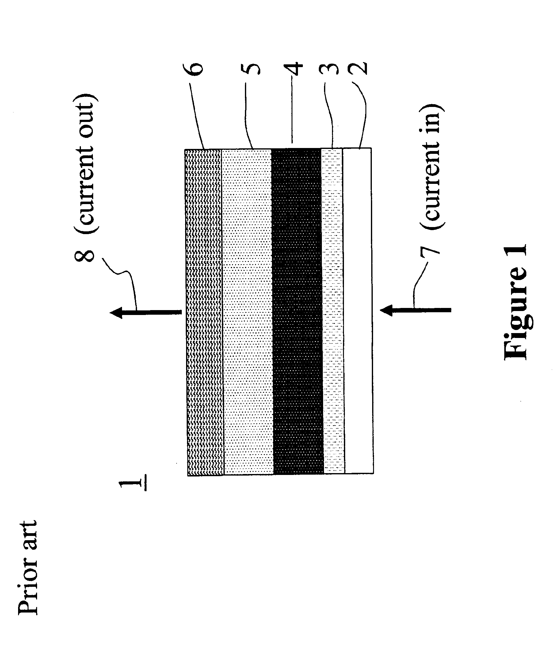
However, the inherent charge mobilities of organic semiconductors are generally much lower than that of inorganic semiconductors, which ultimately results in difficulties in configuring a PN junction device with organic semiconductors.
However, the efficiency and operation stability of these hetrojunction systems are still far below what have been achieved with inorganic semiconductors based devices, not to mention the fabrication complexity of fullerence derivatives or nano-rod of inorganic semiconductors.
This is mainly because of the unsolved fundamental problems with organic semiconductor materials in these systems.
The systems are still in disorder in the nano-scale or the molecular level due to phase separation and discontinuous charge transport media.
The phase separation may cause dimensional instability and performance degradation.
Therefore, how to maximize charge transport and enhance dimensional stability is a critical issue for improve the performance of an organic semiconducting material based device, solar cell in particularly.

Method used


Image

  • Organic semiconductor devices and methods of fabrication
  • Organic semiconductor devices and methods of fabrication
  • Organic semiconductor devices and methods of fabrication

Examples


example 1

Formation of Zeolite Membrane by Steaming Method

[0037]Weigh about 0.610 g of sodium hydroxide pellets and finely grind the pellets with a mortar and pestle. Place this mixture in a 250 ml beaker, and add 2.01 g of water glass containing 40% silica in water and 1.01 g of tetrapropylammonium bromide. Mix with 5.0 ml distilled water, then add 1.0 ml of n-propylamine and mix the solution again.

[0038]Place 1.0 ml of a prepared 1 molar solution of aluminum sulfate along with about 0.05 ml of the concentrated sulfuric acid in a separate 50 ml beaker. Then add the first solution to this beaker as well. Add enough distilled water to raise the volume to about 25 ml, and mix the solution (26 ml total volume) on a stir plate for ten minutes, yield a stable homogeneous dispersion.

[0039]Spin coat the dispersion onto a pre-clean ITO glass to have a gel-like coat layer. Then place the whole part into a stainless steel tube and carefully steam it for 2 hours at a proper pressure.

[0040]After steaming...

example 2

Introduction of Conducting Polymers Precursor into Zeolite Membranes

[0042]The zeolite membrane on ITO glass obtained from example 1 is placed in a glass tube, aniline vapor in nitrogen media is pass through the tube for 4 hours, which introduce aniline molecules into pores of zeolite membrane.

example 3

Formation of Conducting Polymers Inside Zeolite Membranes

[0043]Following example 2, hydrochloric acid vapor in nitrogen media is then passed through the glass tube with the sample obtained in Example 2. This initiates the polymerization of aniline molecules inside zeolite pores and forms conducting polyaniline inside zeolite channels.


PUM

PropertyMeasurementUnit
thicknessaaaaaaaaaa
thicknessaaaaaaaaaa
thicknessaaaaaaaaaa

Abstract

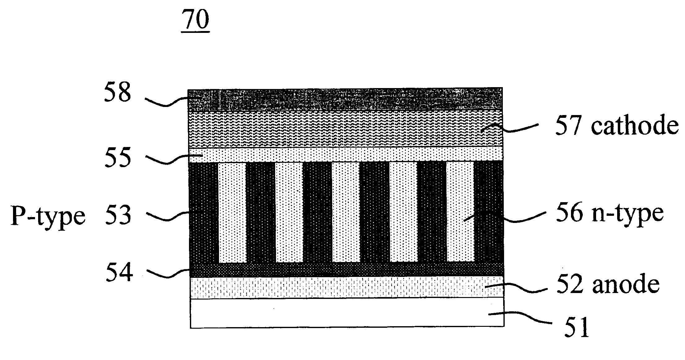
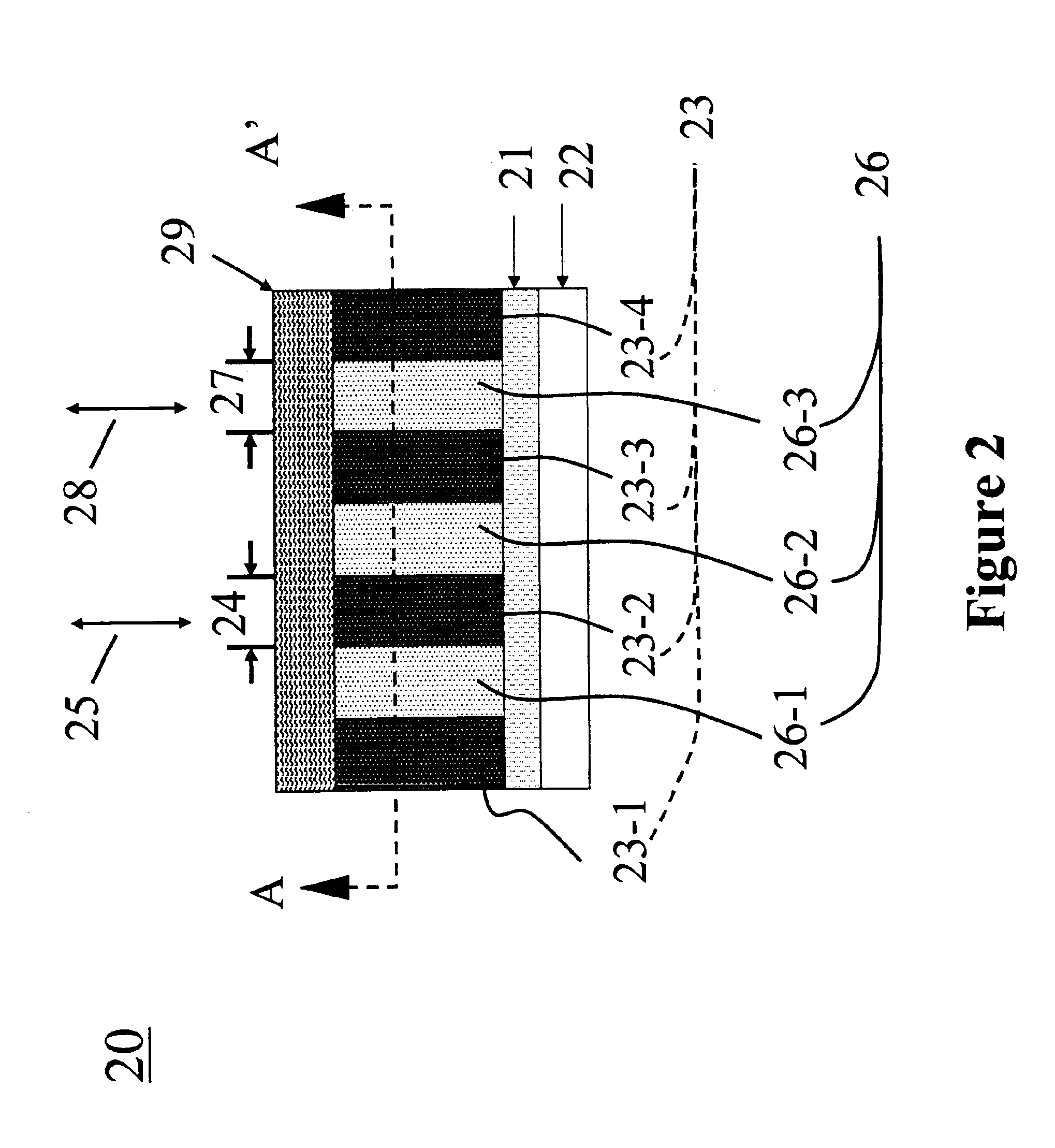
The present invention discloses a vertical junction structure with multi-PN channels, which provides a maximum interface between p-type and n-type materials in order to assist the charge separation, and offers continuous phases in both p- and n-type materials for charge transport in opposite directions.The present invention also provides methods for constructing the device structures. The main steps include 1) assembling a porous structure or a framework with semiconductor materials of one conduction type on a first electrode, 2) filling pores or coating the framework made from the materials in step 1 with semiconductors or precursors of conducting polymer of a opposite conduction type, 3) chemically and physically treating the system to form closed packed multi-PN channels.

Description

FIELD OF THE INVENTION[0001]This invention relates to structures of organic semiconductor devices and the methods of fabrication the same.BACKGROUND OF THE INVENTION[0002]Organic semiconductors, conjugating polymers in particular, have electronic properties of inorganic semiconductors and engineering properties of plastic. They have been employed in many electro-opto applications, including light emitting diodes, solar cells, sensors, transistors and devices for data storage [J. M. Shaw, P. F. Seidler, IBM Journal of Research &Development, 45(1), 3(2001)].[0003]A simple organic semiconductor device may consist of one layer of electro-opto active organic material sandwiched between two electrodes. However, the inherent charge mobilities of organic semiconductors are generally much lower than that of inorganic semiconductors, which ultimately results in difficulties in configuring a PN junction device with organic semiconductors. For example, in configuring a photovoltaic device, an i...

Claims


Application Information

Patent Timeline
Patent Type & Authority Patents(United States)
IPC IPC(8): H01L51/05H01L51/30H01L35/24H01L51/00
CPCH01L51/4246H01L51/0575H01L51/0037H01L51/0038Y02E10/549H10K85/1135H10K85/114H10K10/20H10K30/211H10K30/50
Inventor XIAO, STEVENQIU, CHUNONGQIU, CINDY XING
Owner XIAO STEVEN SHUYONG
Why Eureka
Try Eureka