

Layout method of a comparator array for flash type analog to digital converting circuit
a technology of converting circuit and comparator array, which is applied in the field of layout method of converting circuit of flash-type analog to digital (a/d) converting circuit, can solve the problems of increasing the layout area size and inability to generate accurate digital signals
- Summary
- Abstract
- Description
- Claims
- Application Information
AI Technical Summary
Benefits of technology
Problems solved by technology
Method used
Image

Examples
Embodiment Construction
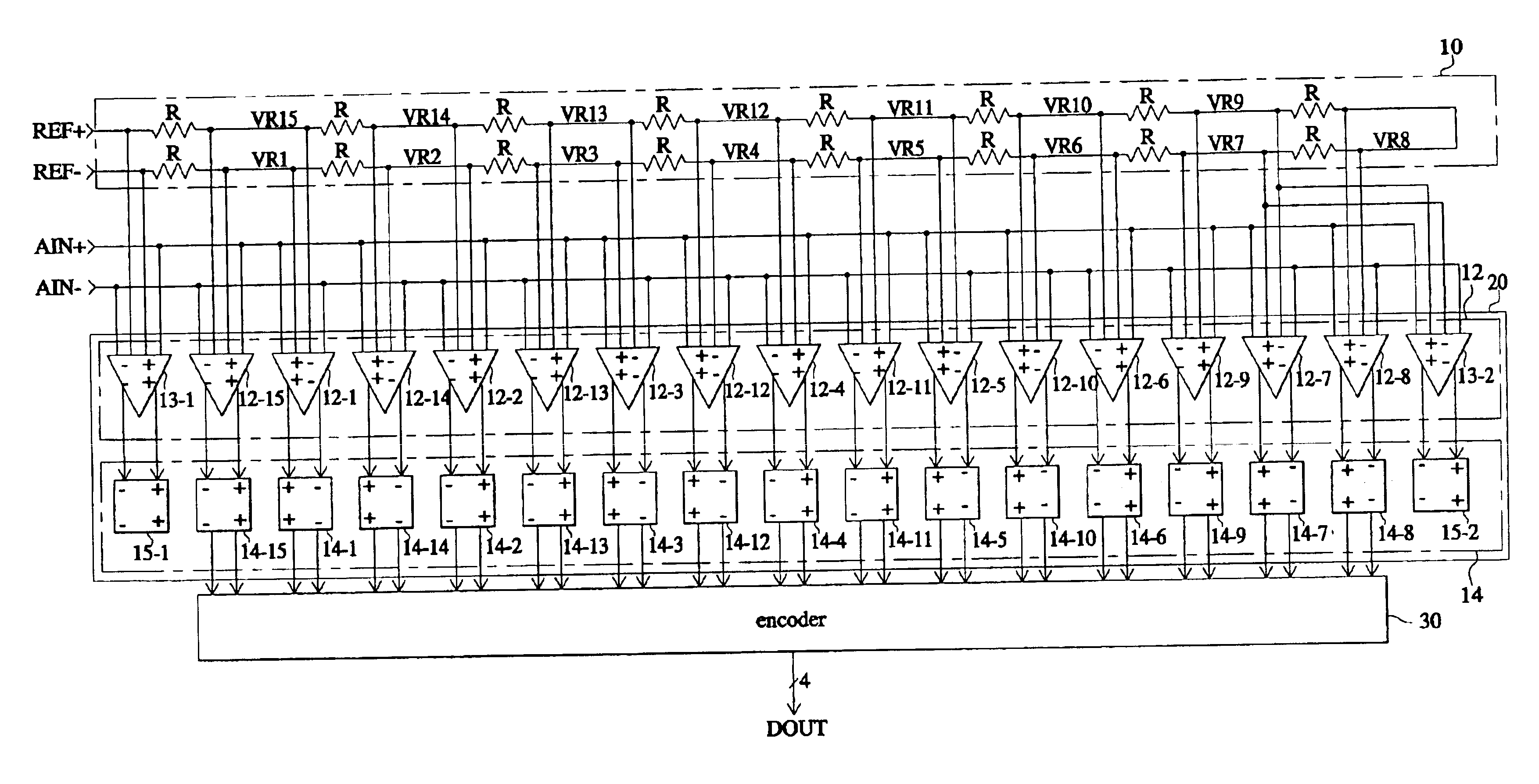
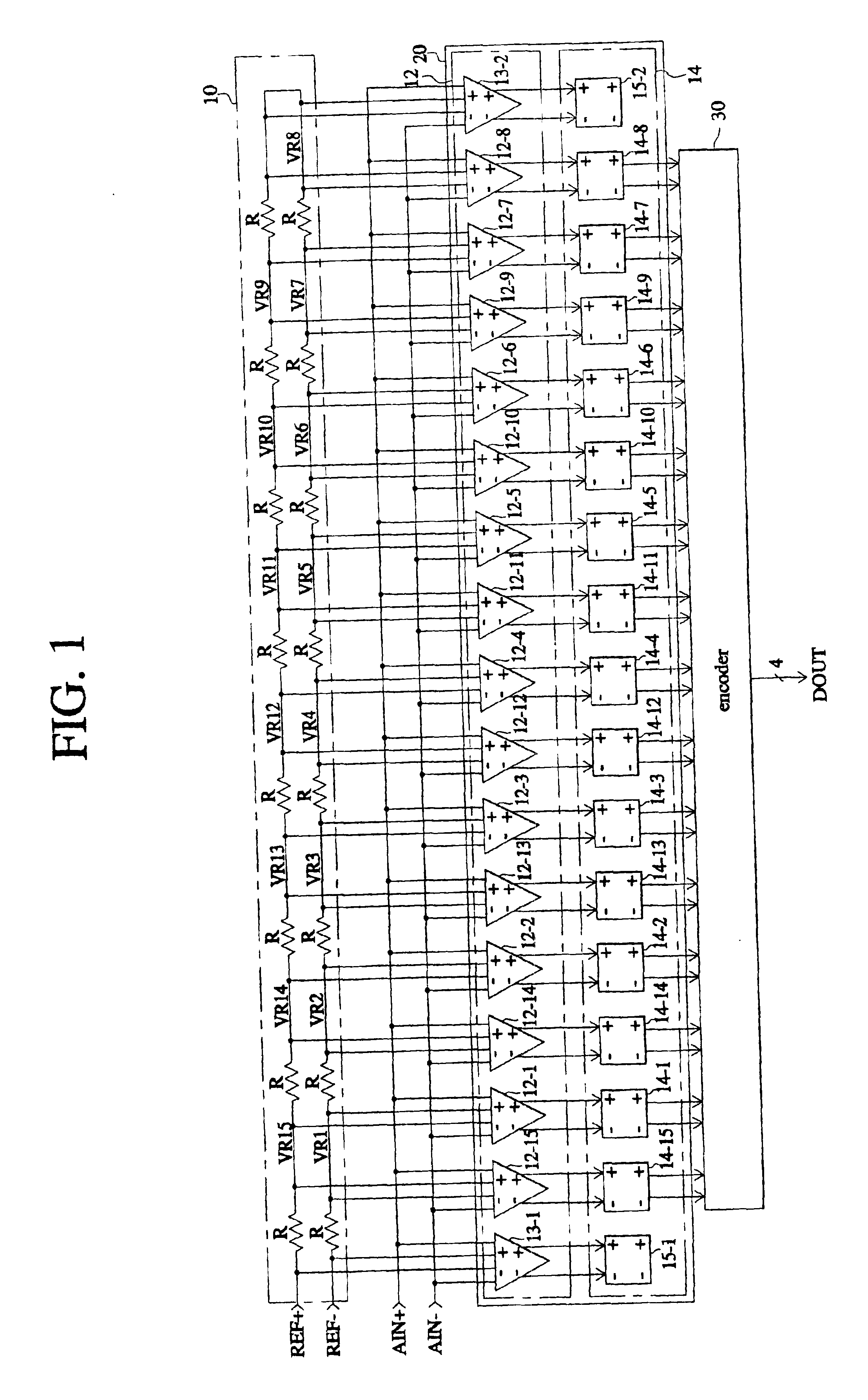
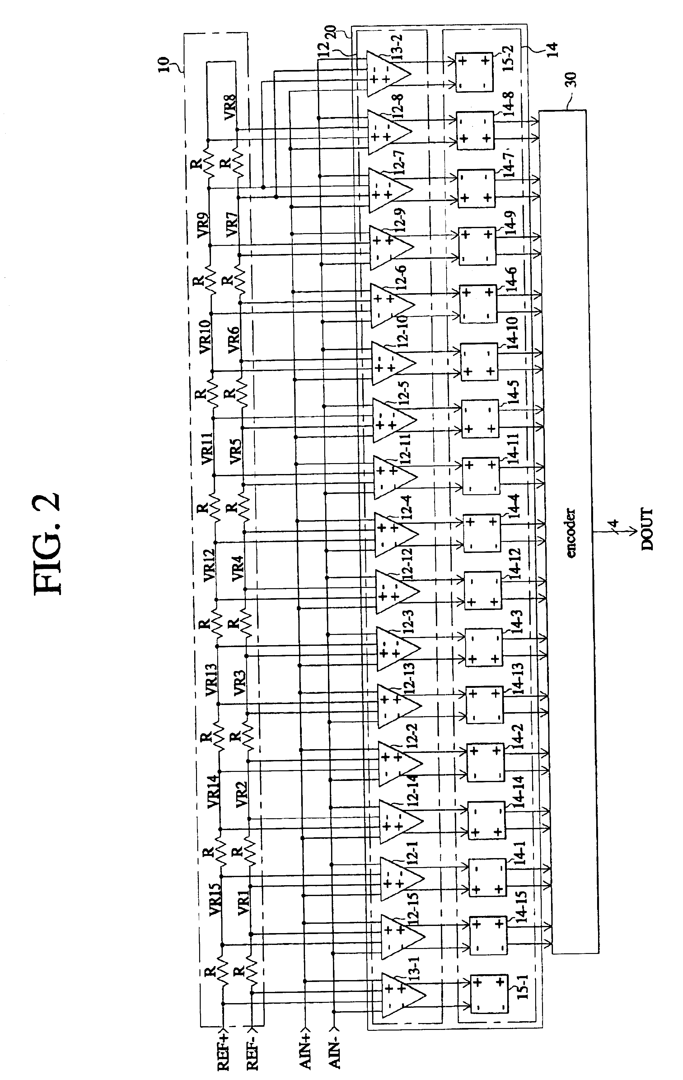
[0024]FIG. 1 is a circuit diagram illustrating a layout of a conventional flash type analog to digital (A / D) converting circuit. The conventional flash type A / D converting circuit of FIG. 1 includes a reference voltage generating circuit 10, a comparator array 20, and an encoder 30.
[0025]As shown in FIG. 1, the reference voltage generating circuit 10 includes 16 resistors which are serially connected between a reference voltage REF+ and a reference voltage REF−. The comparator array 20 includes a pre-amplifying circuit 12 and a latch circuit 14. The pre-amplifying circuit 12 includes 15 pre-amplifiers 12-1 to 12-15 and 2 dummy pre-amplifiers 13-1 and 13-2. The latch circuit 14 includes 15 latches 14-1 to 14-5 and 2 dummy latches 15-1 and 15-2.
[0026]In FIG. 1, a single pre-amplifier and a single of latch constitute a single comparator. A layout of the flash type A / D converting circuit of FIG. 1 is described below.
[0027]The reference voltage (REF+, REF−) terminals and analog signal in...
PUM
 Abstract
Description
Claims
Application Information