Mask and method of manufacturing the same, electro-luminescence device and method of manufacturing the same, and electronic instrument

a manufacturing method and mask technology, applied in the field of masks and manufacturing methods, electroluminescence devices and their manufacturing methods, and electronic instruments, can solve the problems of difficult to manufacture masks with high precision in the conventional method

Inactive Publication Date: 2005-05-17
BOE TECH GRP CO LTD
View PDF22 Cites 13 Cited by
  • Summary
  • Abstract
  • Description
  • Claims
  • Application Information

AI Technical Summary

Problems solved by technology

Though a method in which a base is etched is known as one of the methods of manufacturing a mask, it was difficult to manufacture a mask with high precision in the conventional method.

Method used


Image

  • Mask and method of manufacturing the same, electro-luminescence device and method of manufacturing the same, and electronic instrument
  • Mask and method of manufacturing the same, electro-luminescence device and method of manufacturing the same, and electronic instrument
  • Mask and method of manufacturing the same, electro-luminescence device and method of manufacturing the same, and electronic instrument

Examples


first embodiment

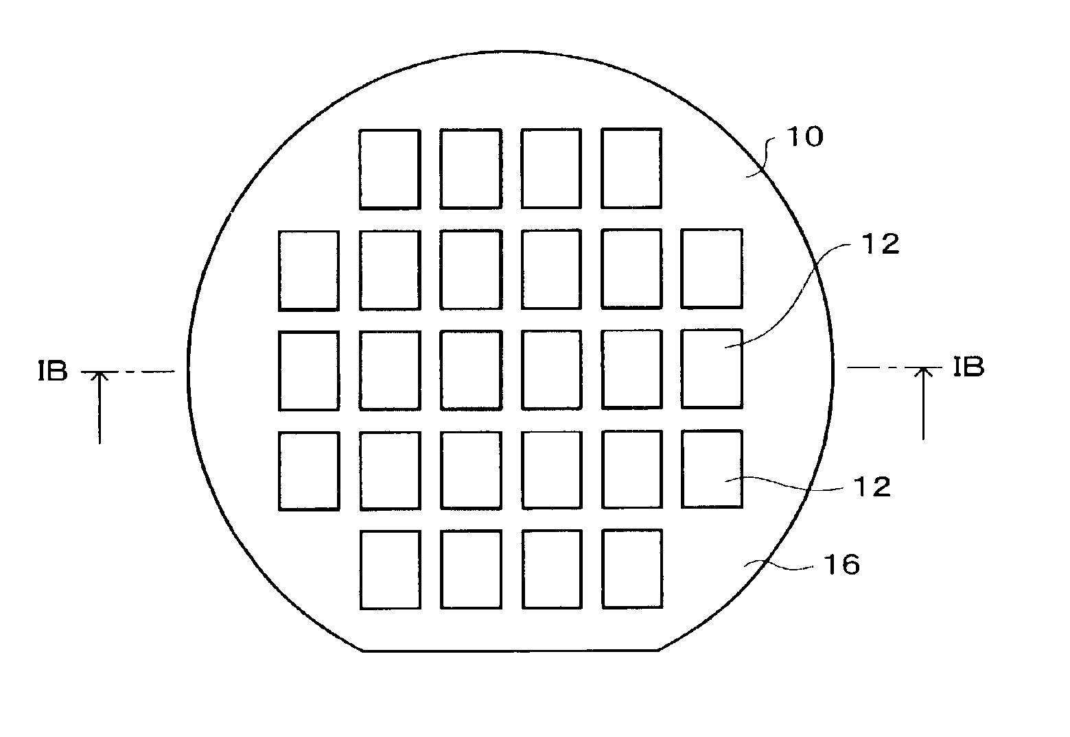
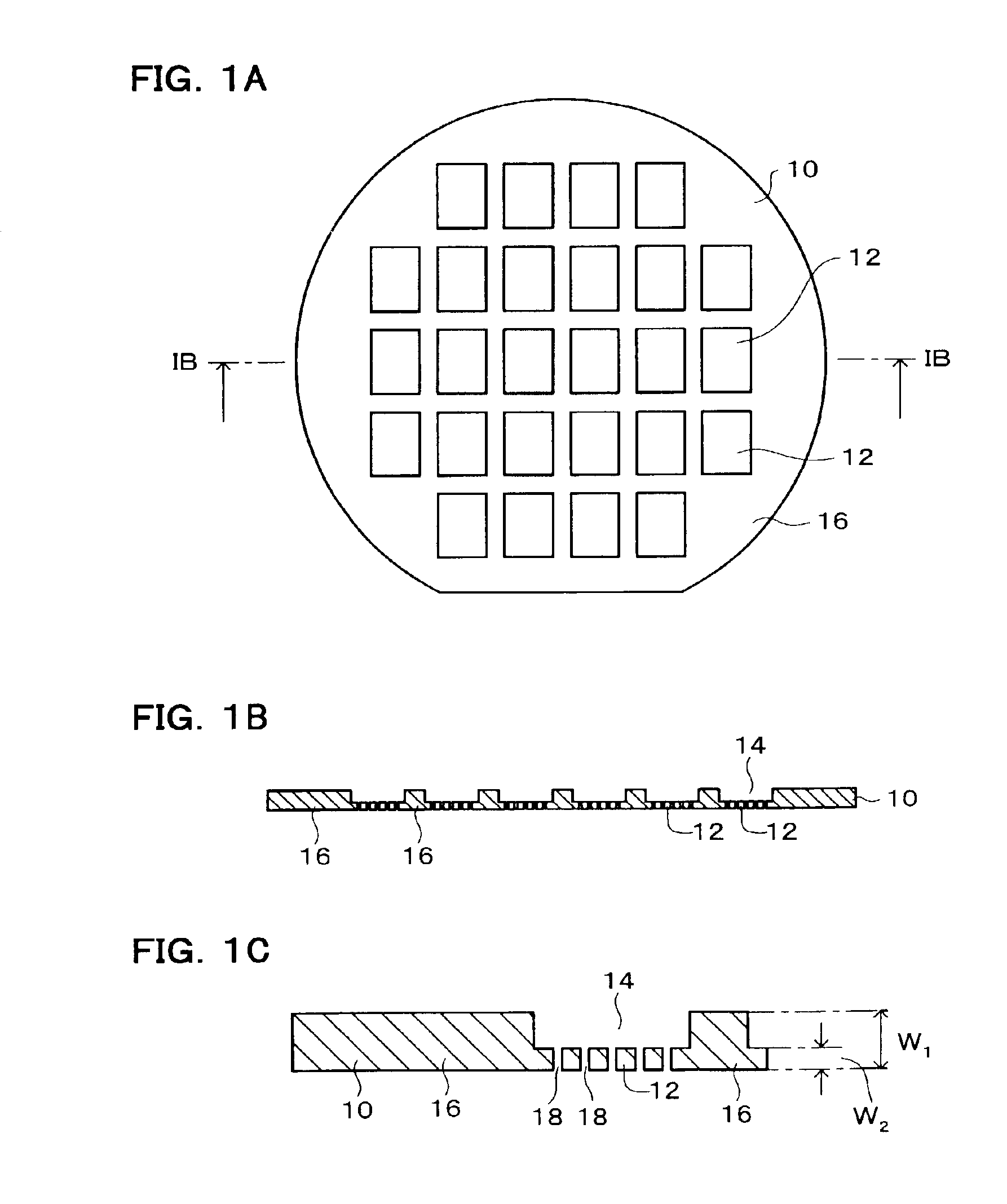
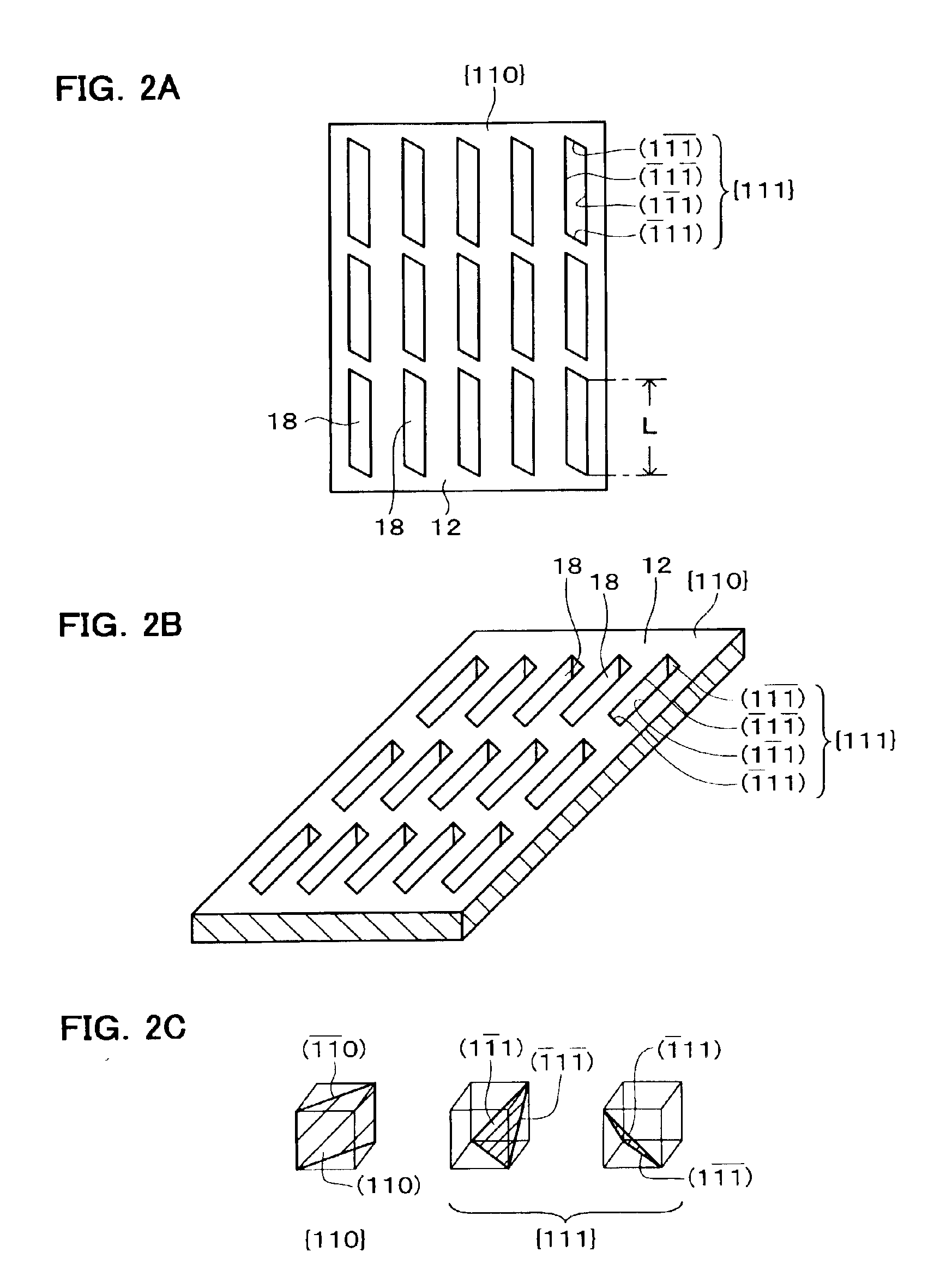
[0106]FIGS. 1A to 1C are diagrams illustrating a mask in accordance with one embodiment of the present invention. FIG. 1B is a sectional view taken along an IB—IB line of FIG. 1A. FIG. 1C is a partially enlarged view of FIG. 1B. The mask has a monocrystal substrate 10 (or is formed by only the monocrystal substrate 10). For example, the monocrystal substrate 10 is a monocrystal silicon substrate, or may be a silicon wafer. The monocrystal substrate 10 has surfaces having Miller indices {110} For example, the top and bottom surfaces of the monocrystal substrate 10 are {110} planes. The {110} planes includes a plurality of planes equivalent to a (110) plane. In a cubic lattice, directions perpendicular to the {110} planes are directions.

[0107]The monocrystal substrate 10 includes at least one (e.g., plural) thin portion 12. A plurality of the thin portions 12 may be provided in a matrix. The monocrystal substrate 10 except the thin portion 12 is a thick portion 16. Strength of the mo...

second embodiment

[0123]FIGS. 4A to 4C are diagrams illustrating a method of manufacturing a mask in accordance with a second embodiment of the present invention. In the first embodiment, the openings 22 are formed in the etching resistant film 20 on opposite surfaces of the monocrystal substrate 10. In this case, since it is difficult to align the positions of the openings 22 on opposite sides, a method for simply aligning these positions will next be mainly explained.

[0124]As shown in FIG. 4A, a first opening 34 is formed in an etching resistant film 30 formed on one surface of the monocrystal substrate 10, and a second opening 36 is formed in an etching resistant film 32 formed on the other surface. Here, the widths A, B of the first and second openings 34, 36 have the relationship: B36 inside a projecting area of the first opening 34. Its positioning is simpler than the alignment of the openings of the same size. Thus, the first opening 34 on one side and the second opening 36 on the other side a...

third embodiment

[0125]FIG. 5 is a diagram illustrating a method of manufacturing a mask in accordance with a third embodiment of the present invention. In the first embodiment, the thickness W1 (see FIG. 1C) of the monocrystal substrate and the length L of a long side of the parallelogram of the opening 22 of the etching resistant film 20 (the same as the length L of alongside of the parallelogram of the penetrating hole 18 shown in FIG. 2A) have the relationship: √3×W1

[0126]In this embodiment, the forming method of the penetrating hole will be explained when the relationship: √3×W1≧L. is formed (when the monocrystal substrate is thick).

[0127]As shown in FIG. 5, a small penetrating hole (a hole smaller than the penetrating hole) 42 is f...


PUM

PropertyMeasurementUnit
crystal orientationaaaaaaaaaa
areaaaaaaaaaaa
shapeaaaaaaaaaa

Abstract

A mask has a monocrystal substrate having opposite surfaces which are planes having Miller indices {110}. A plurality of penetrating holes are formed in the monocrystal substrate. An opening shape of each of the penetrating holes is a polygon and each side of the polygon is parallel with a plane in a group of the {111} planes. The wall surfaces of the penetrating holes are the {111} planes. In the method of manufacturing a mask, openings are formed in the etching resistant film corresponding to the shape of the penetrating holes and the monocrystal substrate is etched.

Description

[0001]Japanese Patent Application No. 2001-287019, filed on Sep. 20, 2001, is hereby incorporated by reference in its entirety.BACKGROUND OF THE INVENTION[0002]The present invention relates to a mask and its manufacturing method, an electro-luminescence device and its manufacturing method, and an electronic instrument.[0003]A mask with high precision is required. For example, a method of manufacturing a color organic electro-luminescence (hereinafter called EL) device that is known uses a mask to deposit an organic material of each color. Though a method in which a base is etched is known as one of the methods of manufacturing a mask, it was difficult to manufacture a mask with high precision in the conventional method.BRIEF SUMMARY OF THE INVENTION[0004]According to a first aspect of the present invention, there is provided a method of manufacturing a mask comprising:[0005]forming an etching resistant film having a plurality of openings having a polygonal shape on surfaces of a mon...

Claims


Application Information

Patent Timeline
Patent Type & Authority Patents(United States)
IPC IPC(8): C30B33/00G03F7/12G03F1/16H01L51/56H01L51/50H05B33/10C23C14/04G03F1/20H05B33/12
CPCC30B33/00H01L51/56G03F7/12G03F1/20H10K71/00H05B33/10
Inventor YOTSUYA, SHINICHI
Owner BOE TECH GRP CO LTD
Why Eureka
Try Eureka