Method for evaluating degree of crystalline orientation of polycrystalline silicon, method for selecting polycrystalline silicon rod, polycrystalline silicon rod, polycrystalline silicon ingot, and method for manufacturing monocrystalline silicon

a technology of polycrystalline silicon and crystalline orientation, applied in the direction of silicon compounds, material analysis using wave/particle radiation, instruments, etc., can solve the problems of induction of dislocation generation, loss of crystal lines, defect formation, etc., and achieve the effect of stable manufacturing of monocrystalline silicon

Active Publication Date: 2016-03-01
SHIN ETSU CHEM IND CO LTD
View PDF35 Cites 3 Cited by
  • Summary
  • Abstract
  • Description
  • Claims
  • Application Information

AI Technical Summary

Benefits of technology

[0021]A polycrystalline silicon rod selected by the method of the present invention is a “non-oriented” rod low in the degree of crystalline orientation. Accordingly, the local generation of partial unmelted residues is prevented if crystal growth is carried out by an FZ method using such a polycrystalline silicon rod or if crystal growth is carried out by a CZ method using a polycrystalline silicon ingot obtained by crushing the polycrystalline silicon rod. Thus, it is possible to stably manufacture monocrystalline silicon.

Problems solved by technology

Thus, these polycrystalline pieces may be a cause for the induction of dislocation generation and the loss of crystal lines.
In addition, in Patent Literature 2, there is pointed out a problem in which acicular crystal may deposit within a polycrystalline silicon rod (polycrystalline silicon bar) in a process for manufacturing the rod by a Siemens method and, if monocrystalline silicon is grown by an FZ method using such a polycrystalline silicon rod, individual crystallites do not melt uniformly according to their sizes due to the abovementioned non-uniform microstructure, and unmelted crystallites pass through a melt zone as solid particles into a monocrystalline rod as unmelted particles to be incorporated into coagulated surfaces of a monocrystal, thus causing defect formation.

Method used


Image

  • Method for evaluating degree of crystalline orientation of polycrystalline silicon, method for selecting polycrystalline silicon rod, polycrystalline silicon rod, polycrystalline silicon ingot, and method for manufacturing monocrystalline silicon
  • Method for evaluating degree of crystalline orientation of polycrystalline silicon, method for selecting polycrystalline silicon rod, polycrystalline silicon rod, polycrystalline silicon ingot, and method for manufacturing monocrystalline silicon
  • Method for evaluating degree of crystalline orientation of polycrystalline silicon, method for selecting polycrystalline silicon rod, polycrystalline silicon rod, polycrystalline silicon ingot, and method for manufacturing monocrystalline silicon

Examples


examples

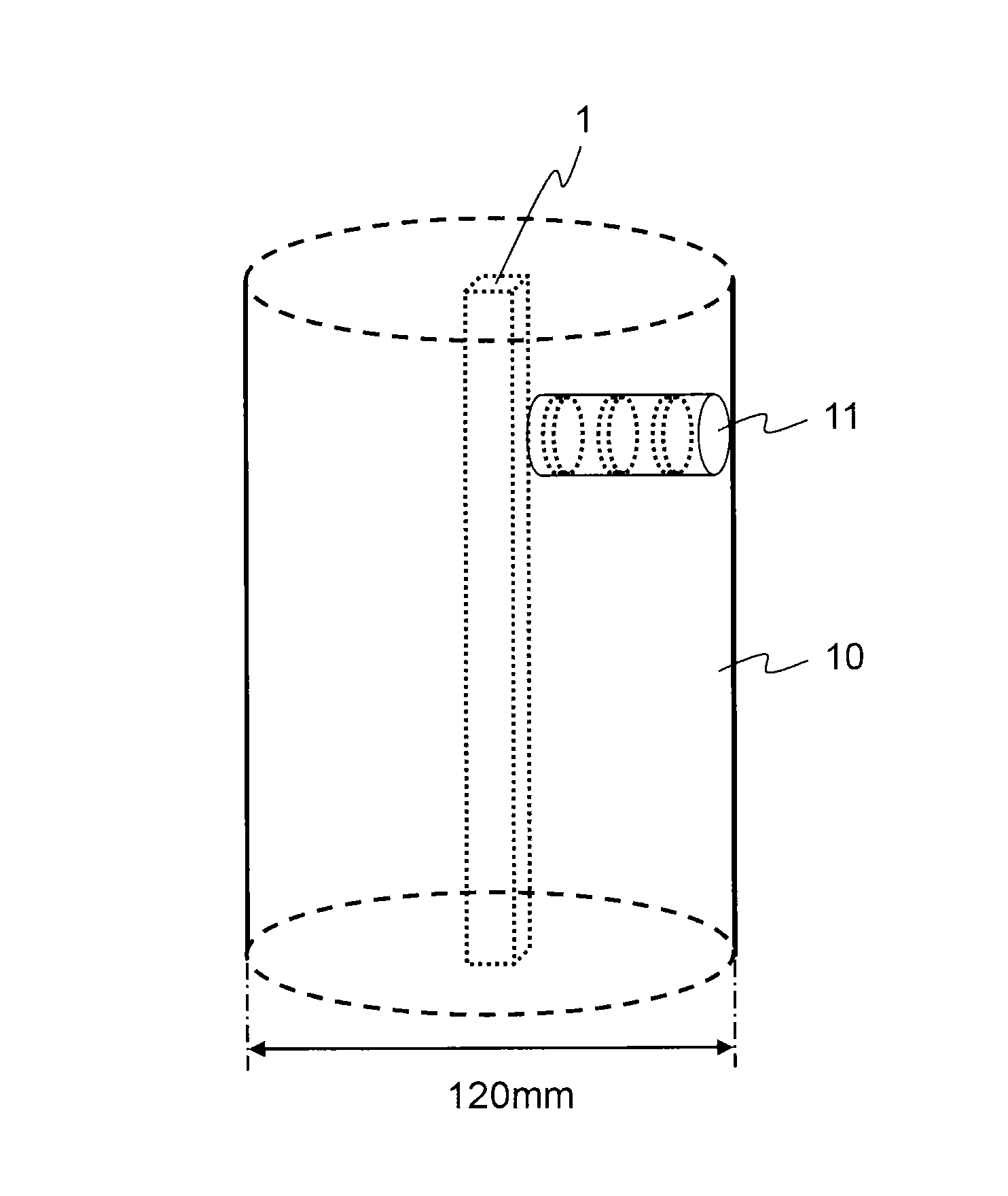
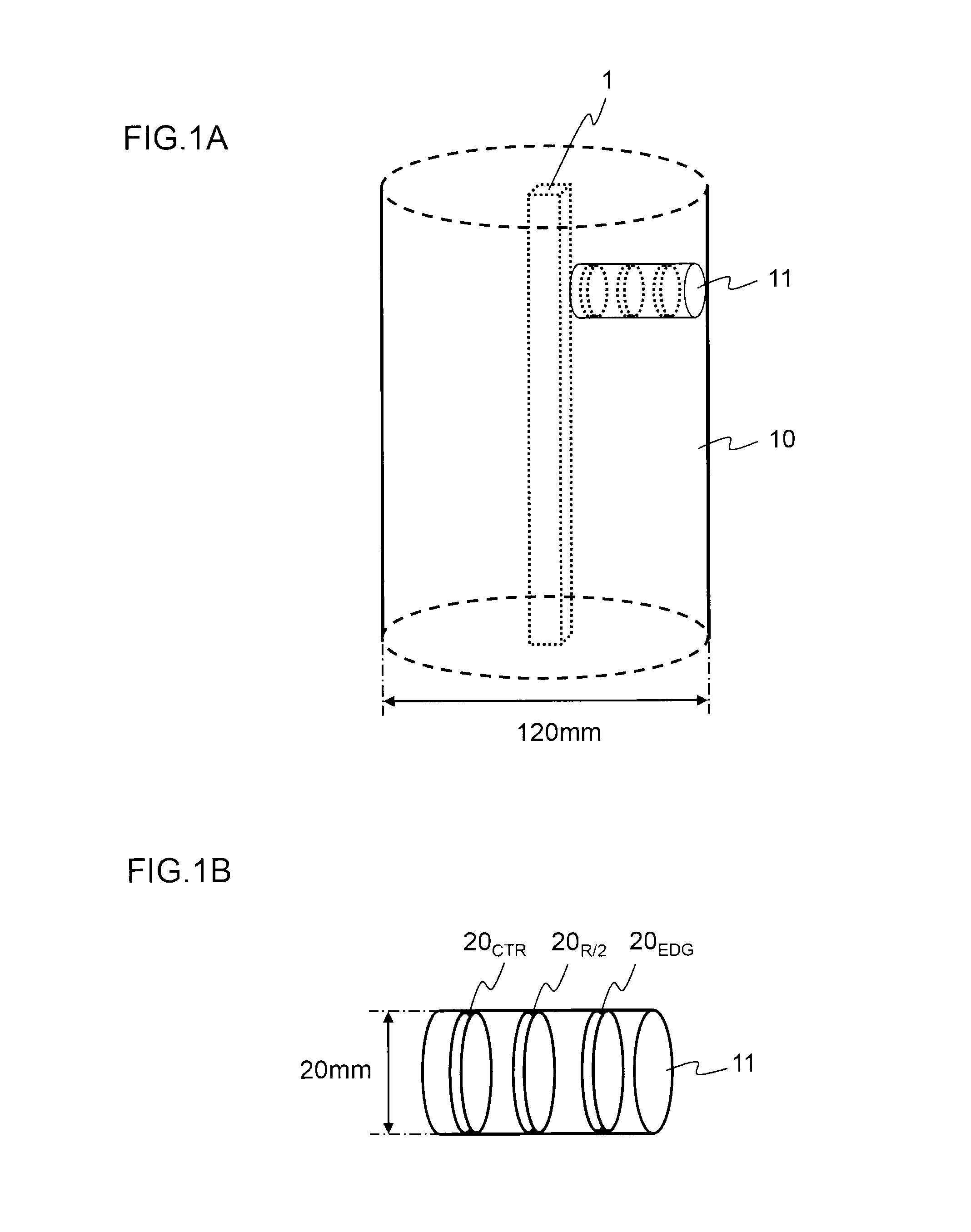
[0065]Six polycrystalline silicon rods grown under different deposition conditions were prepared. Approximately 2 mm-thick disc-like samples (20CTR, 20EDG and 20R / 2) were taken from the three locations illustrated in FIGS. 1A and 1B for each of these polycrystalline silicon rods (silicon rods A to F). Using the measurement system illustrated in FIG. 6, φ-scan charts of Miller index faces and were obtained. Note that the diameter of the disc-like samples 20 is approximately 20 mm.

[0066]Table 1 summarizes the diffraction intensity of a baseline (BL) for each of the disc-like samples obtained from these polycrystalline silicon rods and the presence / absence of the loss of crystal lines when monocrystalline silicon rods were grown by an FZ method using the polycrystalline silicon rods.

[0067]

TABLE 1Plate-BL IntensitySiliconlike(kcps)Max / MinDivision ValueLoss ofRodSampleI<111>I<220>I<111> / I<220>Crystal LinesA20CTR6.84.01.461.431.70No20R / 28.04.81.6720EDG9.95.71.74B...


PUM

PropertyMeasurementUnit
diameteraaaaaaaaaa
lengthaaaaaaaaaa
diameteraaaaaaaaaa

Abstract

When the degree of crystalline orientation of polycrystalline silicon is evaluated by an X-ray diffraction method, each obtained disc-like sample 20 is disposed in a position where Bragg reflection from a Miller index face <hkl> is detected and in-plane rotated at a rotational angle φ with the center of the disc-like sample 20 as the center of rotation, so that an X-ray-radiated region defined by a slit φ-scans over the principal surface of the disc-like sample 20, to determine a chart representing the dependence of the intensity of Bragg reflection from the Miller index face <hkl> on the rotational angle (φ) of the disc-like sample 20, a baseline is determined from the chart, and the diffraction intensity value of the baseline is used as an estimative index of the degree of crystalline orientation.

Description

TECHNICAL FIELD[0001]The present invention relates to a method for evaluating the degree of crystalline orientation of polycrystalline silicon, and a method for selecting a suitable non-orientational polycrystalline silicon rod or ingot as a raw material for stably manufacturing monocrystalline silicon utilizing the evaluating method.BACKGROUND ART[0002]Monocrystalline silicon essential for the manufacture of semiconductor devices and the like is grown by a CZ method or an FZ method, and a polycrystalline silicon rod or a polycrystalline silicon ingot is used as a raw material at that time. Such polycrystalline silicon materials are manufactured by a Siemens method in most cases (see, for example, Patent Literature 1). The Siemens method is a method for bringing a silane raw material gas, such as trichlorosilane or monosilane, into contact with a heated silicon core wire to vapor phase-grow (deposit) polycrystalline silicon on the surfaces of the silicon core wire by a CVD (Chemical...

Claims


Application Information

Patent Timeline
Patent Type & Authority Patents(United States)
IPC IPC(8): C30B29/06C30B29/60C01B33/02C30B13/00C01B33/21G01N23/20G01N23/207C01B33/021C01B33/035
CPCG01N23/20C01B33/02C01B33/021C01B33/035C30B13/00C30B29/06C30B29/605G01N23/207G01N2223/3306G01N2223/606
Inventor MIYAO, SHUICHIOKADA, JUNICHINETSU, SHIGEYOSHI
Owner SHIN ETSU CHEM IND CO LTD
Why Eureka
Try Eureka