Advanced RF enhancement-mode FETs with improved gate properties

a technology of enhancement mode and gate property, which is applied in the direction of semiconductor devices, electrical apparatus, transistors, etc., can solve the problems of poor gate property, prone to excessive current leakage, and increase in the size and weight of the system or devi

Inactive Publication Date: 2005-05-17
NXP USA INC
View PDF17 Cites 123 Cited by
  • Summary
  • Abstract
  • Description
  • Claims
  • Application Information

AI Technical Summary

Problems solved by technology

This, in turn, has required the presence of a positive and negative power source, resulting in an increase in the size and weight of the system or device.
While enhancement mode HFETs of the type depicted in FIG. 1 have many desirable properties, these devices are frequently found to exhibit a forward turn-on voltage of the gate diode (VON) that is unexpectedly lower than the design value.
Many of these devices are found to be prone to excessive current leakage and poor gate properties, as well as excessive contact and access resistances.

Method used


Image

  • Advanced RF enhancement-mode FETs with improved gate properties
  • Advanced RF enhancement-mode FETs with improved gate properties
  • Advanced RF enhancement-mode FETs with improved gate properties

Examples


Embodiment Construction

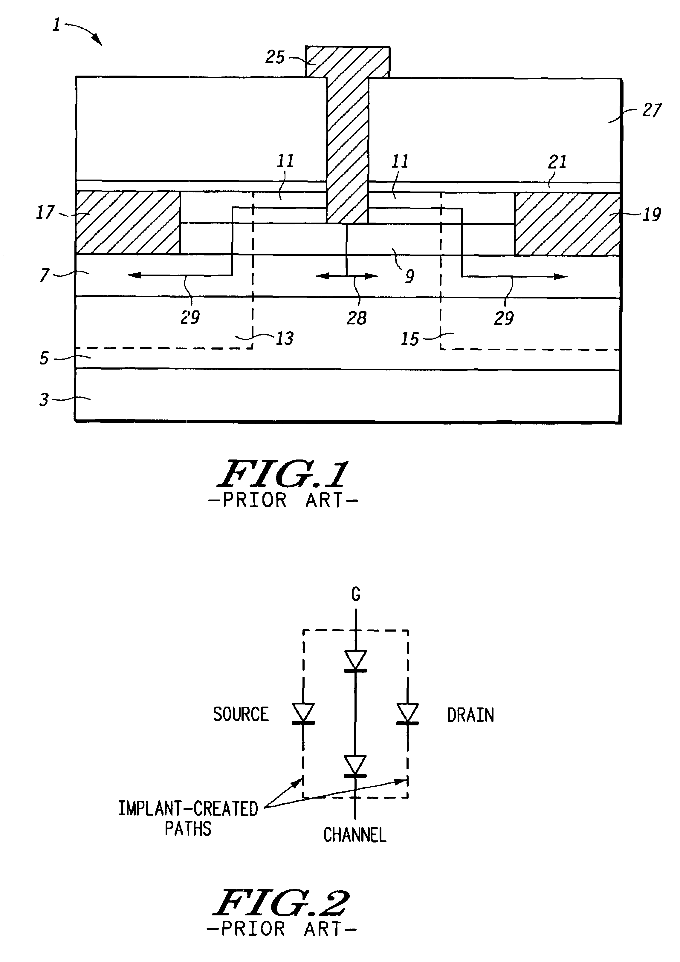
[0015]Surprisingly, it has now been found that the aforementioned problems frequently encountered in enhancement mode HFETs can arise from the overlap of the cap layer with the implant regions in these devices. As indicated by arrows 29 in FIG. 1, the implantation process used to form the source and drain regions results in the formation of alternative leakage paths between the gate and channel, in addition to the main leakage path indicated by arrow 28. Hence, as indicated schematically in the illustration of FIG. 2, the cumulative result of these additional paths is to lower the VON of the device, resulting in excessive current leakage.

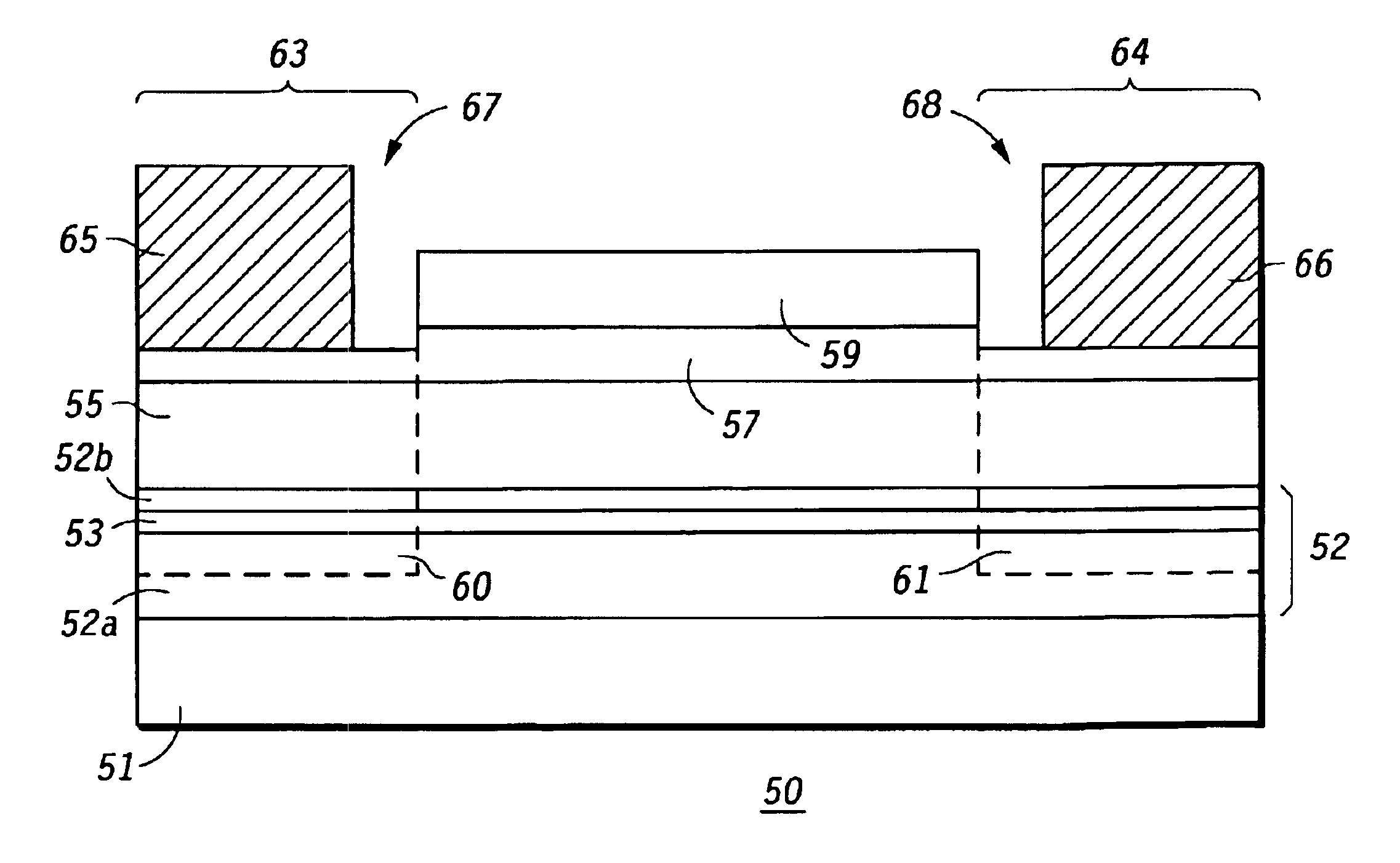
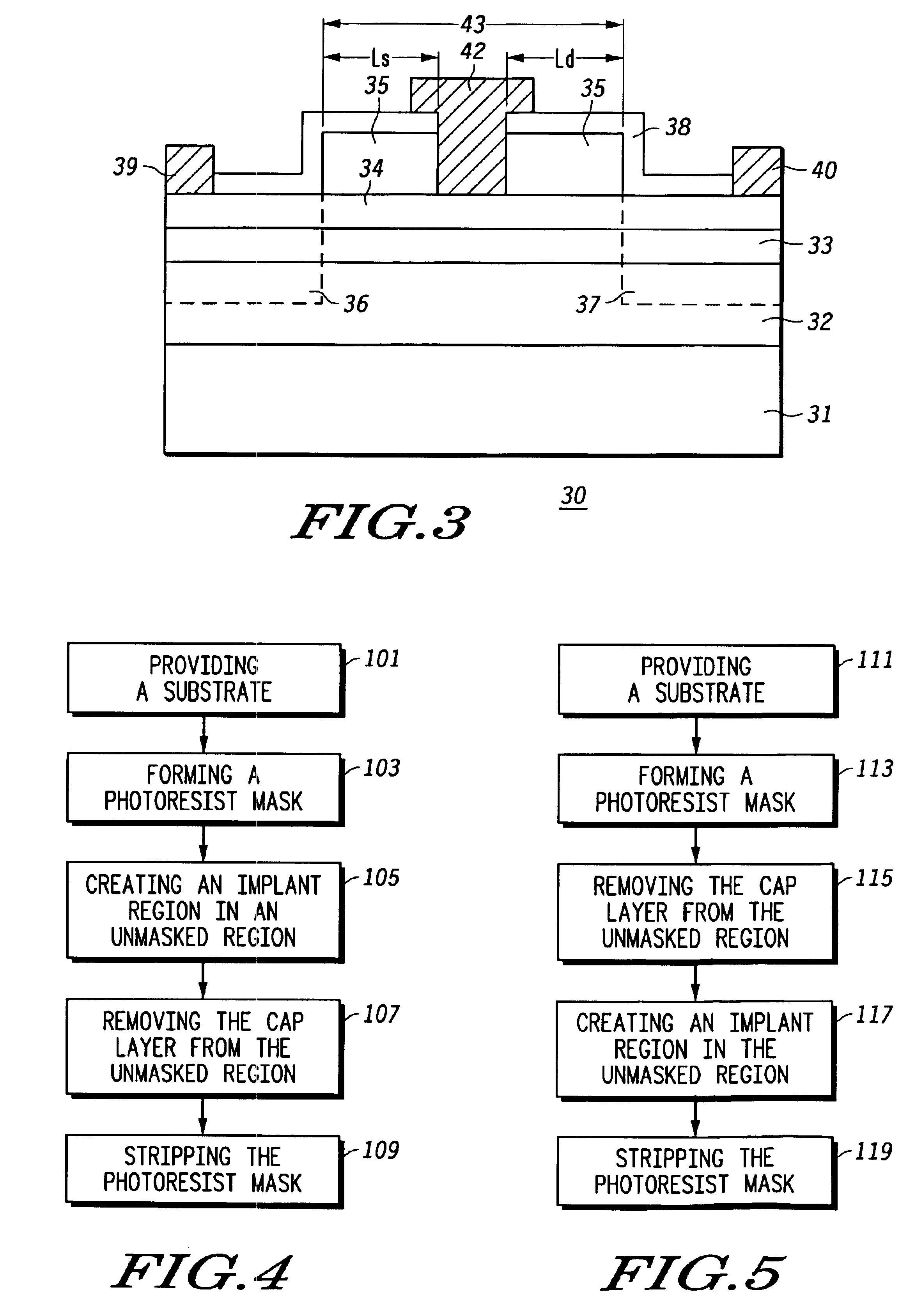
[0016]FIG. 3 shows a simplified cross-sectional view of one particular example of an enhancement mode HFET that can be made in accordance with the teachings herein and that does not suffer from the infirmities of the device of FIG. 1. The device 30 of FIG. 3 is formed on a wafer 31 and includes a buffer layer 32 formed on the upper surface of the wa...


PUM


Abstract

A method for fabricating an RF enhancement mode FET (30) having improved gate properties is provided. The method comprises the steps of providing (131) a substrate (31) having a stack of semiconductor layers (32-35) formed thereon, the stack including a cap layer (35) and a central layer (33) defining a device channel, forming (103) a photoresist pattern (58) over the cap layer, thereby defining a masked region and an unmasked region, and, in any order, (a) creating (105) an implant region (36, 37) in the unmasked region, and (b) removing (107) the cap layer from the unmasked region. By forming the implant region and cap region with no overlap, a device with low current leakage may be achieved.

Description

FIELD OF THE INVENTION[0001]The present invention relates generally to methods for fabricating enhancement mode RF devices, and more particularly to methods for making enhancement mode FETs with improved gate properties.BACKGROUND OF THE INVENTION[0002]HFETs (Heterojunction Field Effect Transistors) have found use in mobile telephones and other communications systems and devices. Such devices have often been used in depletion mode, thus requiring the application of a positive bias to the drain electrode and a negative bias to the gate electrode. This, in turn, has required the presence of a positive and negative power source, resulting in an increase in the size and weight of the system or device. Consequently, it has become desirable in these applications to replace the depletion mode HFET with an enhancement mode HFET, which does not require the application of a negative bias to the gate electrode or the accompanying devices required to achieve that bias.[0003]FIG. 1 shows a simpl...

Claims


Application Information

Patent Timeline
Patent Type & Authority Patents(United States)
IPC IPC(8): H01L21/285H01L21/02H01L21/337H01L29/66H01L29/80
CPCH01L21/28587H01L29/802H01L29/66924
Inventor MARTINEZ, MARINO J.SCHIRMANN, ERNESTHARTIN, OLIN L.RAMPLEY, COLBY G.SADAKA, MARIAM G.WEITZEL, CHARLES E.COSTA, JULIO
Owner NXP USA INC
Why Eureka
Try Eureka