LDMOS transistor capable of attaining high withstand voltage with low on-resistance and having a structure suitable for incorporation with other MOS transistors

a technology of mos transistor and ldmos, which is applied in the direction of transistors, semiconductor devices, electrical devices, etc., can solve the problems of low withstand voltage, inferiority to vdmos (vertical double-diffused metal oxide semiconductor) transistors, and drain region misalignment, so as to improve the stability of ldmos, reduce the on-resistance of mos, and reduce the on-resistance of ldmos

Active Publication Date: 2005-05-17
RICOH KK
View PDF11 Cites 29 Cited by
  • Summary
  • Abstract
  • Description
  • Claims
  • Application Information

AI Technical Summary

Benefits of technology

[0023]In one example, the mitigation oxide layer is not diffused in a portion between the source region and the drain region. Thus, a current flows from the source region to the drain region without being interrupted, thereby lowering on-resistance of the LDMOS.
[0048]In another example, the channel well region is thermally diffused in the twelfth step, before forming the second source and drain regions in the fifteenth step or before implanting the first gate electrode in the sixteenth step. In this way, redistribution of the channel well region is prevented.

Problems solved by technology

LDMOS transistors particularly have a simple structure suitable for incorporation into the VLSI logic circuits, however, they have been considered inferior to VDMOS (vertical double-diffused metal oxide semiconductor) transistors as they have high on-resistance.
However, the above-described manufacturing method easily causes misalignment of the drain region 123, which is desirably formed apart from the gate electrode 117 for high withstand voltage.
However, this may cause low withstand voltage.
Any one of the above-described or other background LDMOS transistors has another problem, when manufactured with other MOS transistors.
This may cause the withstand voltage of the other MOS transistors to decrease.

Method used


Image

  • LDMOS transistor capable of attaining high withstand voltage with low on-resistance and having a structure suitable for incorporation with other MOS transistors
  • LDMOS transistor capable of attaining high withstand voltage with low on-resistance and having a structure suitable for incorporation with other MOS transistors
  • LDMOS transistor capable of attaining high withstand voltage with low on-resistance and having a structure suitable for incorporation with other MOS transistors

Examples


Embodiment Construction

[0062]In describing preferred embodiments illustrated in the drawings, specific terminology is employed for the sake of clarity. However, the disclosure of this patent specification is not intended to be limited to the specific terminology so selected and it is to be understood that each specific element includes all technical equivalents that operate in a similar manner. Referring now to the drawings, wherein like reference numerals designate identical or corresponding parts throughout the several views, preferred embodiments of the present invention are explained.

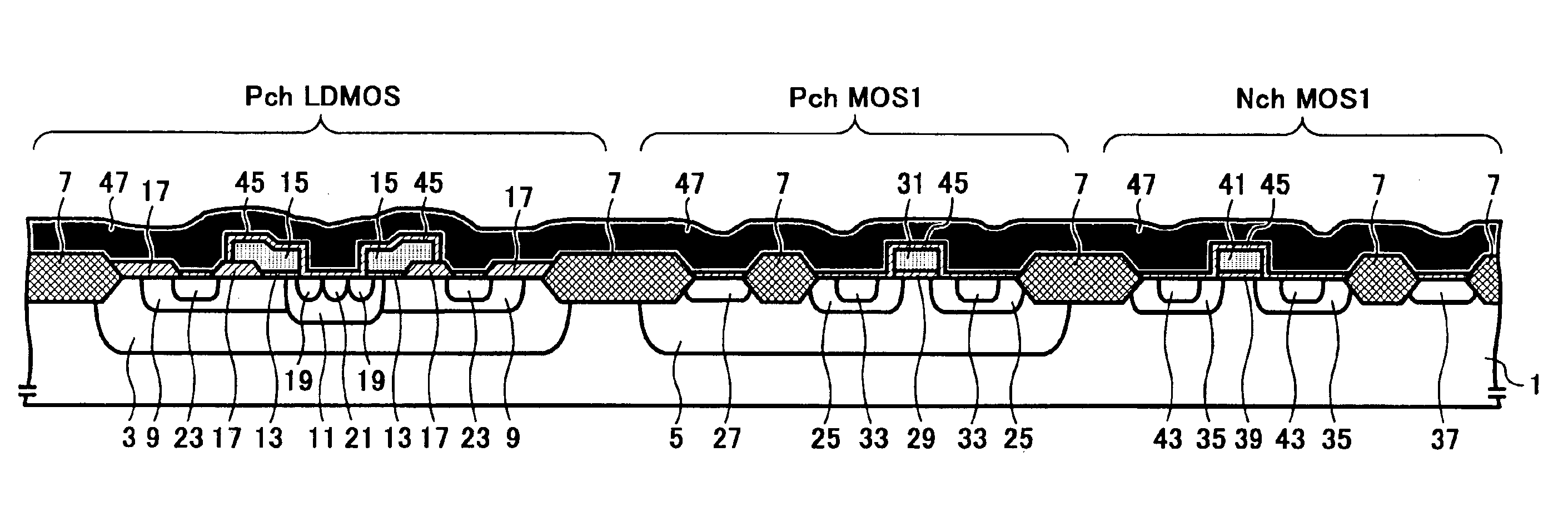
[0063]FIG. 5I illustrates a section of a semiconductor device according to an embodiment of the present invention. The semiconductor device of FIG. 5I includes a P-channel LDMOS transistor (hereinafter, referred to as a “PchLDMOS”), and a CMOS transistor provided with a P-channel MOS transistor (hereinafter, referred to as a “PchMOS1”) and an N-channel MOS transistor (hereinafter, referred to as an “NchMOS1”), all of whic...


PUM


Abstract

A semiconductor device, methods for manufacturing the semiconductor device, and an integrated circuit including the semiconductor device are disclosed. The semiconductor device includes an LDMOS transistor and a MOS transistor, both formed simultaneously on a same substrate. The gate electrodes and the gate oxide layers of the LDMOS and the MOS are formed independently from one another. The source and drain regions of the LDMOS and the MOS are respectively formed in a self-aligned manner. In this way, the LDMOS and the MOS can be formed, in an effective manner, while sustaining the respective desired characteristics.

Description

CROSS-REFERENCE TO RELATED APPLICATIONS[0001]This application claims priority to Japanese patent application, No. JPAP2003-201672 filed on Jul. 25, 2003, in the Japanese Patent Office, the entire contents of which are incorporated by reference herein.FIELD OF THE INVENTION[0002]The present invention relates to a semiconductor device, methods for manufacturing the semiconductor device, and an integrated circuit including the semiconductor device, and more particularly, to a semiconductor device incorporating an LDMOS (lateral double-diffused metal oxide semiconductor) transistor, methods for manufacturing a semiconductor device incorporating an LDMOS transistor, and an integrated circuit including a semiconductor device incorporating an LDMOS transistor.BACKGROUND OF THE INVENTION[0003]Recently, with the widespread use of VLSI (very large scale integration), power control integrated circuits are generally provided with power devices, VLSI logic circuits, memory devices, CPUs (central...

Claims


Application Information

Patent Timeline
Patent Type & Authority Patents(United States)
IPC IPC(8): H01L21/70H01L21/8234H01L21/8238H01L27/085H01L27/088H01L27/092H01L29/94H01L29/78
CPCH01L21/823814H01L21/82385H01L21/823857H01L27/0922H01L29/7835H01L29/66659H01L29/66681H01L29/7816H01L29/42368H01L21/22H01L2924/13091
Inventor SHIMIZU, AKIRANEGORO, TAKAAKI
Owner RICOH KK
Why Eureka
Try Eureka