Non-volatile memory with phase-change recording layer

a phase-change recording and non-volatile memory technology, applied in nanoinformatics, instruments, record information storage, etc., can solve the problems of insufficient large amount of electric power needed to write or delete data, and difficult to save power, so as to increase the possible number of data rewriting cycles and reduce power consumption.

Inactive Publication Date: 2005-05-31
PANASONIC CORP
View PDF6 Cites 139 Cited by
  • Summary
  • Abstract
  • Description
  • Claims
  • Application Information

AI Technical Summary

Benefits of technology

[0009]The present invention aims to solve these problems and to provide a non-volatile memory that can increase the possible number of data rewriting cycles while lowering power consumption, and the fabrication method thereof.

Problems solved by technology

However, when the joint portion 81a is insulated using silicon oxide, which is an inorganic dielectric having a relatively high thermal conductivity, a large amount of electric power is needed to write or delete data.
This makes it difficult to save power.
However, when using only an organic dielectric as the material for the insulating layer 84, the number of data rewriting cycles is insufficient because the heat withstand temperature of the organic dielectric is lower than the melting point of the phase-change material.

Method used


Image

  • Non-volatile memory with phase-change recording layer
  • Non-volatile memory with phase-change recording layer
  • Non-volatile memory with phase-change recording layer

Examples


Embodiment Construction

[0042]Embodiments of the present invention will be described below with reference to the accompanying drawings.

(Non-volatile Memories)

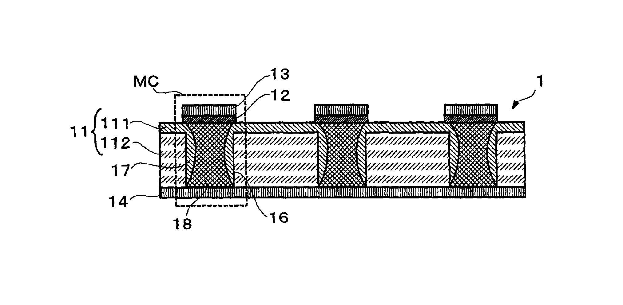
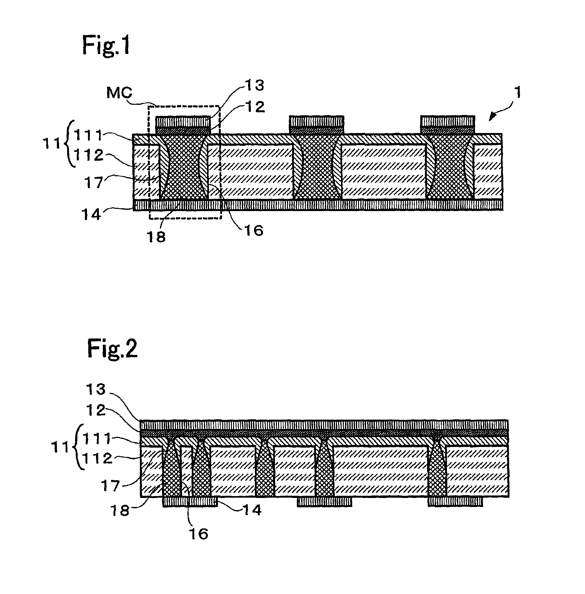
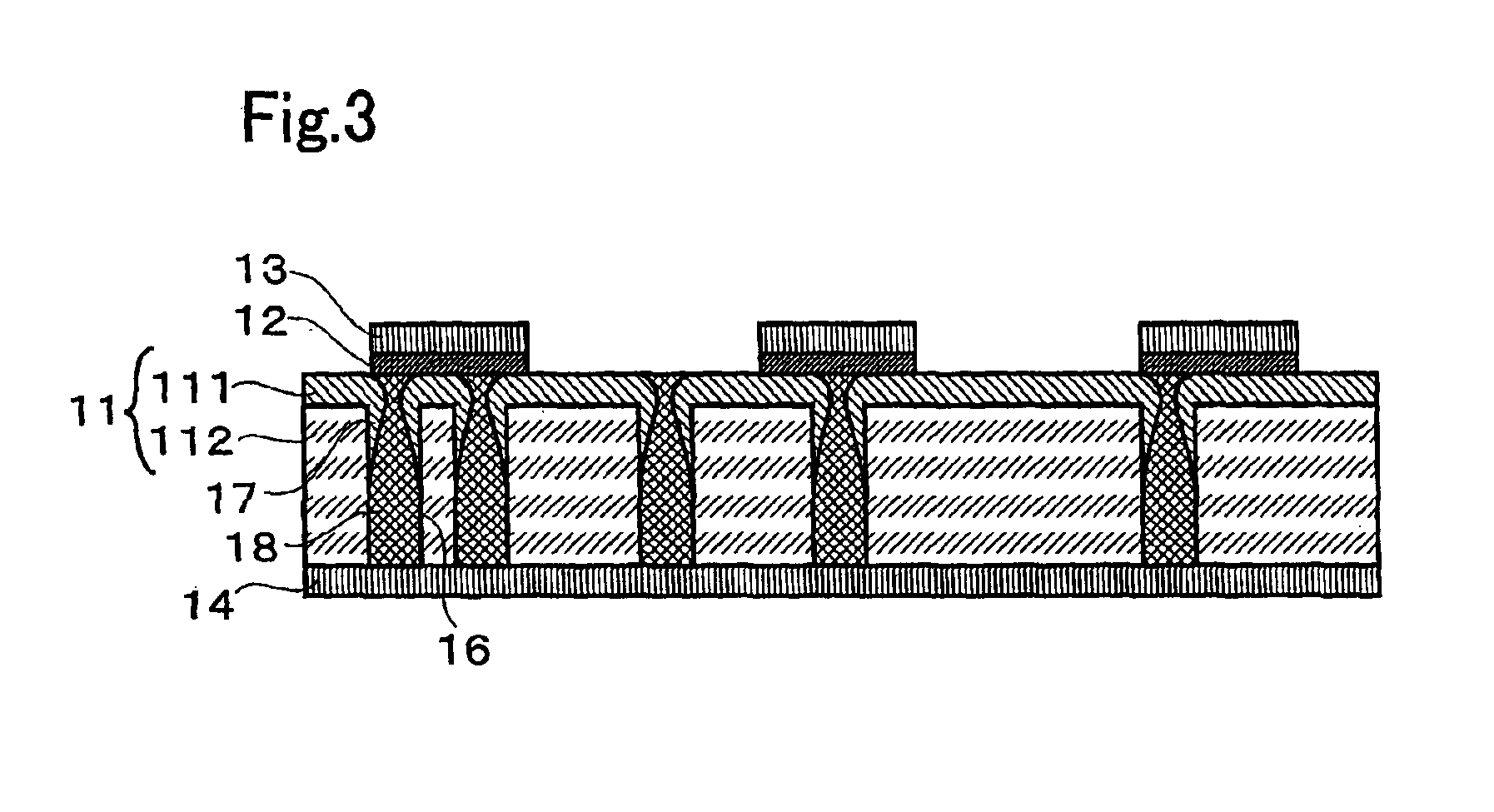
[0043]FIG. 1 is a cross-sectional view showing the main parts of a non-volatile memory according to one embodiment of the present invention. As shown in FIG. 1, a non-volatile memory 1 comprises an insulating substrate 11 that is formed by laminating an inorganic dielectric layer 111 and an organic dielectric thin film 112, recording layers 12 and upper electrodes 13 that are formed on the inorganic dielectric layer 111 side of the insulating substrate 11, and a lower electrode 14 that is formed on the organic dielectric thin film 112 side of the insulating substrate 11.

[0044]The inorganic dielectric layer 111 is formed of an insulator that is inert to the recording layer 12 during heat generation, and can be an oxide film of SiOx and the like, a nitride film of SiNx and the like, as well as SiO2—ZnS, SiO2—ZnSe, etc. For example, when the inorganic di...


PUM

PropertyMeasurementUnit
thicknessaaaaaaaaaa
thicknessaaaaaaaaaa
aspect ratioaaaaaaaaaa

Abstract

A non-volatile memory, which comprises an insulating substrate (11) that has a first electrode (18) that extends through the substrate from the front surface to the rear surface thereof; a second electrode (13) that is formed on one side of the insulating substrate (11); and a recording layer (12) that is clamped between the first electrode (18) and the second electrode (13) and whose resistance value varies when an electric pulse is applied across the first electrode (18) and the second electrode (13); wherein the insulating substrate (11) has a layered structure composed of an organic dielectric thin film (112) and an inorganic dielectric layer (111) that is thinner than the organic dielectric thin film (112); with the recording layer (12) being formed on the side on which the inorganic dielectric layer is formed. Use of this non-volatile memory increases the possible number of data writing cycles while saving power.

Description

[0001]This application is a continuation-in-part of PCT / JP03 / 04066, filed Mar. 31, 2003.TECHNICAL FIELD[0002]The present invention relates to a non-volatile memory, and more particularly to a non-volatile memory in which data can be recorded (written) or deleted by using the application of current to control resistance value variations, and to the fabrication method thereof.BACKGROUND ART[0003]Flash memory, FeRAM, MRAM, phase-change memory, and the like are conventionally known types of non-volatile memory. Recent years have brought about a demand for high-density memories for use in personal digital assistants and the like, and therefore non-volatile memories that employ a phase-change technique are attracting widespread attention and various modifications to them have been proposed (WO, A1 No. 98 / 19350 (Japanese Unexamined Patent Publication No. 2001-502848), etc.).[0004]For example, Japanese Unexamined Patent Publication No. 1997-282723 discloses an information-recording device i...

Claims


Application Information

Patent Timeline
Patent Type & Authority Patents(United States)
IPC IPC(8): G11C16/02G11C11/22H01L27/24G11B9/00G11B9/04H01L45/00H01L27/10
CPCB82Y10/00H01L45/1273G11B9/14G11B9/1409G11B9/1418G11B9/1463G11B9/149G11C11/22G11C13/0004H01L27/101H01L45/06H01L45/1233H01L45/144H01L45/16H01L27/2472G11B9/04H10B63/82H10N70/8418H10N70/231H10N70/011H10N70/8828H10N70/826
Inventor TANAKA, HIDEYUKIMORIMOTO, KIYOSHI
Owner PANASONIC CORP
Why Eureka
Try Eureka