Semiconductor display device and manufacturing method thereof

a technology of semiconductors and display devices, applied in the field of semiconductor display devices, can solve the problems of large reliability problems, deterioration phenomena, and decreased drain curren

Inactive Publication Date: 2005-06-21
SEMICON ENERGY LAB CO LTD
View PDF115 Cites 15 Cited by
  • Summary
  • Abstract
  • Description
  • Claims
  • Application Information

AI Technical Summary

Benefits of technology

[0051]Next, low concentration ion implantation of an n-type or p-type impurity is performed for the semiconductor layer 102 comprising the polycrystalline silicon film corresponding to a region in which the first layer gate electrode 104 is exposed. By the low concentration ion implantation of the n-type or p-type impurity, low concentration impurity regions (n− regions or p− regions) 108 as the Lov regions are formed. In this case, since a mask for the ion implantation comprises the negative resist pattern 107 and the second layer gate electrode 105 having a thick film thickness, it has extremely high blocking performance against the implanted ion. Thus, when an accelerating voltage and the amount of ions to be implanted at the time of ion implantation are suitably selected, an impurity with a suitable concentration can be independently ion-implanted by through dope into only the semiconductor layer 102 corresponding to the exposed region of the first layer gate electrode 104 (see FIG. 1C).
[0061]Also, according to the present invention, in the case where the GOLD structure polycrystalline silicon TFT having both the Lov regions and the Loff regions is formed, ion implantation into the Lov regions is independently performed using a negative resist pattern formed in a self alignment by the rear surface exposure method as a mask, whereby impurity concentrations of the Lov regions and the Loff regions can be independently controlled. Therefore, the GOLD structure polycrystalline silicon TFT having both the hot carrier resistance and the off-current suppressing effect can be formed.

Problems solved by technology

However, when the polycrystalline silicon TFT is continuously driven, there is the case where a deterioration phenomenon such as a reduction in a mobility or an on-current (current flowing in the case where the TFT is in an on-state) and an increase in an off-current (current flowing in the case where the TFT is in an off-state) is observed.
This is a large problem in reliability.
However, since the resistance of the low concentration impurity regions (n− regions) is large, there is such a defect that a drain current is decreased.
Thus, a deterioration mode inherent to the LDD, such as the low concentration impurity regions (n− regions) are depleted and the resistance is increased becomes a problem.
As a channel length is shortened, the above problems are come to be apparent.
Thus, although an effect for suppressing the off-current is large, there is such a defect that an effect for suppressing a hot carrier by relaxing the electric field near the drain is small.
However, there is such a defect that the off-current becomes large.
However, since a manufacturing process is complicated, an increase in a manufacturing cost and a reduction in a yield become a large problem.

Method used


Image

  • Semiconductor display device and manufacturing method thereof
  • Semiconductor display device and manufacturing method thereof
  • Semiconductor display device and manufacturing method thereof

Examples


embodiment mode 1

[Embodiment Mode 1]

[0079]A method of forming a GOLD structure polycrystalline silicon TFT having both Lov regions and Loff regions will be described based on FIGS. 3A to 3H.

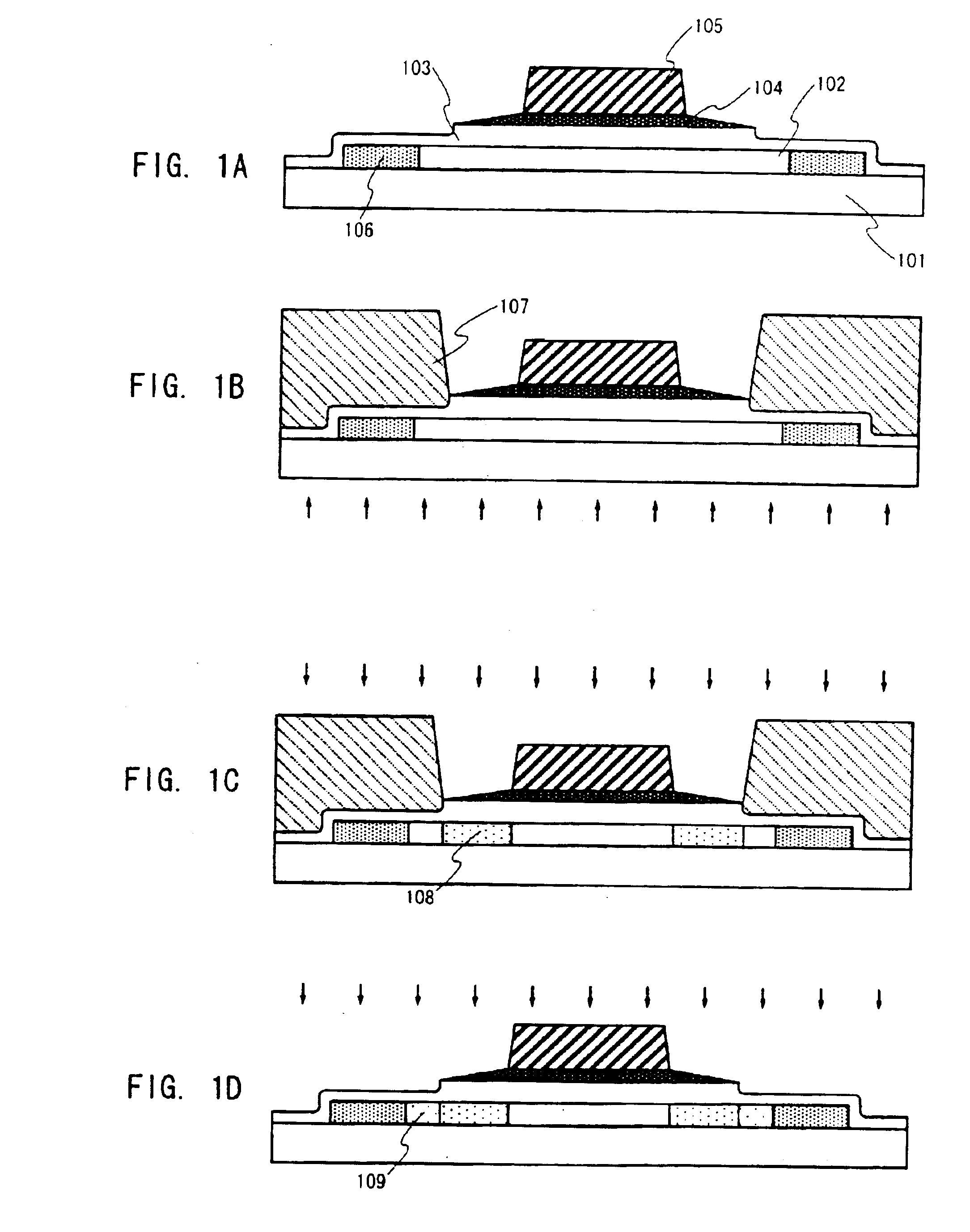
[0080]With respect to a substrate structure used in this embodiment mode, a semiconductor layer 202 comprising a polycrystalline silicon film, a gate insulating film 203, a first layer gate electrode film 204, and a second layer gate electrode film 205 are laminated to have respective predetermined film thicknesses on a glass substrate 201. On the substrate having such a structure, a resist pattern 206 for forming a gate electrode is formed (see FIG. 3A).

[0081]Next, a first step in dry etching processing is performed using the above resist pattern 206 as a mask. By the dry etching processing for a predetermined period, only the second layer gate electrode film 205 is isotropy-etched to form a second layer gate electrode 208 with a taper shape. In this case, with respect to the resist pattern 206 used as the mask ...

embodiment mode 2

[Embodiment Mode 2]

[0090]Another method of forming a GOLD structure polycrystalline silicon TFT having both Lov regions and Loff regions will be described based on FIGS. 4A to 4H. Although this embodiment mode is substantially similar to Embodiment mode 1, there is a slight difference in a method of forming a gate electrode. Therefore, this point will be described as the emphasis.

[0091]With respect to a substrate structure used in this embodiment mode, a semiconductor layer 302 comprising a polycrystalline silicon film, a gate insulating film 303, a first layer gate electrode film 304, and a second layer gate electrode film 305 are laminated at respective predetermined film thicknesses on a glass substrate 301. On the substrate having such a structure, a resist pattern 306 for forming a gate electrode is formed (see FIG. 4A).

[0092]Next, a first step and a second step in dry etching processing are performed in succession using the above resist pattern 306 as a mask to form a first la...

embodiment 1

[Embodiment 1]

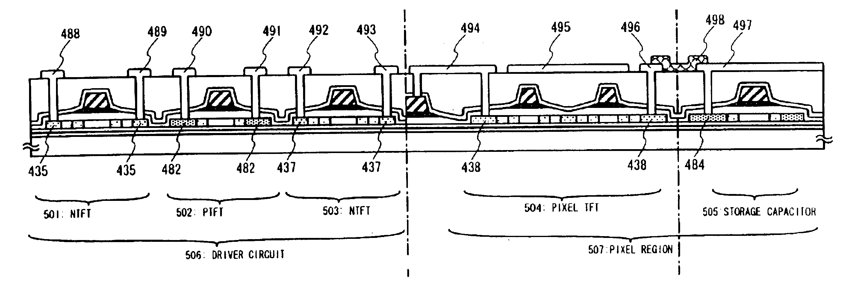
[0099]A method of manufacturing an active matrix liquid crystal display comprising a GOLD structure polycrystalline silicon TFT having both Lov regions and Loff regions will be concretely described based on FIGS. 5A and 5B to 11.

[0100]First, a silicon oxynitride silicon film 402a of a first layer having a film thickness of 50 nm and a silicon oxynitride film 402b of a second layer having a film thickness of 100 nm, which have different composition ratios are deposited on a glass substrate 401 by a plasma CVD method to form a base film 402. Note that, as a material of the glass substrate 401 used here, there is quartz glass, barium borosilicate glass, aluminoborosilicate glass, or the like. Next, after an amorphous silicon film is deposited to have a thickness of 55 nm on the above base film 402 (402a and 402b) by a plasma CVD method, a solution containing nickel is kept on the amorphous silicon film. After this amorphous silicon film is dehydrogenated (500° C. and 1 ho...


PUM

PropertyMeasurementUnit
temperatureaaaaaaaaaa
sizeaaaaaaaaaa
thicknessaaaaaaaaaa

Abstract

A semiconductor display device which includes the polycrystalline silicon TFTs is constructed by a pixel region and a peripheral circuit and TFT characteristics required for each circuit are different. For example, an LDD structure TFT having a large off-current suppressing effect is suitable for the pixel region. Also, a GOLD structure TFT having a large hot carrier resistance is suitable for the peripheral circuit. When the performance of the semiconductor display device is improved, it is suitable that difference TFT structures are used for each circuit. In the case where the GOLD structure TFT having both Lov regions and Loff regions is formed, ion implantation into the Lov regions is independently performed using a negative resist pattern formed in a self alignment by a rear surface exposure method as a mask, and thus impurity concentrations of the Lov regions and the Loff regions can be independently controlled. Therefore, the GOLD structure TFT having both the hot carrier resistance and the off-current suppressing effect can be formed and the simplification of a manufacturing process of the semiconductor display device and the improvement of performance thereof are compatible with each other.

Description

[0001]This application is a divisional of U.S. application Ser. No. 09 / 957,915, filed on Sep. 21, 2001 now U.S. Pat. No. 6,562,671.BACKGROUND OF THE INVENTION[0002]1. Field of the Invention[0003]The present invention relates to a semiconductor display device having a circuit comprising thin film transistors (hereinafter referred to as TFTs) and a manufacturing method thereof. As the semiconductor display device, there is an electro-optical device such as a liquid crystal display and an EL (electroluminescence) display, which comprises, for example, the TFTs.[0004]2. Description of the Related Art[0005]Recently, an active matrix liquid crystal display technique using the TFT is noted. An active matrix display is superior to a passive matrix display in a response speed, a view angle, and a contrast. Thus, this currently becomes the mainstream of a note type personal computer, a liquid crystal television, or the like.[0006]The TFT is generally constructed using amorphous silicon or pol...

Claims


Application Information

Patent Timeline
Patent Type & Authority Patents(United States)
IPC IPC(8): H01L29/786H01L21/70H01L29/423H01L21/84H01L29/66H01L29/49H01L29/40H01L27/12G02F1/13G02F1/1362H01L21/77
CPCH01L27/1214H01L29/42384H01L29/78621H01L29/78627H01L29/78675H01L29/4908G02F1/13454H01L2029/7863H01L27/1288
Inventor OHNUMA, HIDETO
Owner SEMICON ENERGY LAB CO LTD
Why Eureka
Try Eureka