Transparent conductive optical sheet having high invisibility of pattern

A transparent conductive, optical sheet technology, applied in optics, optical components, electrical digital data processing, etc., can solve problems such as trouble, poor surface resistance, and reduced effect of film dryness

Active Publication Date: 2016-04-27
爱思开迈克沃解决方案有限公司
View PDF3 Cites 4 Cited by
  • Summary
  • Abstract
  • Description
  • Claims
  • Application Information

AI Technical Summary

Problems solved by technology

[0005] However, the existing transparent conductive optical sheets still have room for improvement in terms of optical, electrical, and mechanical properties.
[0006] In particular, the surface resistance required by this transparent conductive optical sheet will be different according to different electronic products to be installed. In order to achieve this surface resistance, when changing the deposition thickness of the ITO layer, the film between the refractive index matching layer The effect of the dr

Method used


Image

  • Transparent conductive optical sheet having high invisibility of pattern
  • Transparent conductive optical sheet having high invisibility of pattern
  • Transparent conductive optical sheet having high invisibility of pattern

Examples


Embodiment 1 to 20

[0147] Examples 1 to 20: Fabrication of Transparent Conductive Optical Sheets with Index Matching Layers

[0148] Step 1: Prepare the transparent base layer

[0149] A PET transparent substrate having a refractive index of 1.63 to 1.67 in a wavelength of 550 nm and a thickness of 50 μm was used.

[0150] Step 2: Forming the first index matching layer

[0151] 5.5 parts by weight of thermosetting acrylic resin (A811, Ai Jing Chemical Co.), 0.3 parts by weight of polyisocyanate curing agent (DN980S, Ai Jing Chemical Company), 47.1 parts by weight of xylene (xylene) for dilution and After 47.1 parts by weight of butyl acetate are mixed, 50 to 80 parts by weight of zirconia (ZrO 2 , JGC Corporation) for further mixing. Then, the obtained mixed solution is wet-coated on the transparent base layer, and then dried and thermally cured, so as to form the first layer having a refractive index in the range of 1.56-1.66 at a wavelength of 550 nm and a thickness in the range of 20-100 n...

Embodiment 11 to 35

[0190] Examples 11 to 35: Transparent conductive optical sheet with hardness-enhancing film

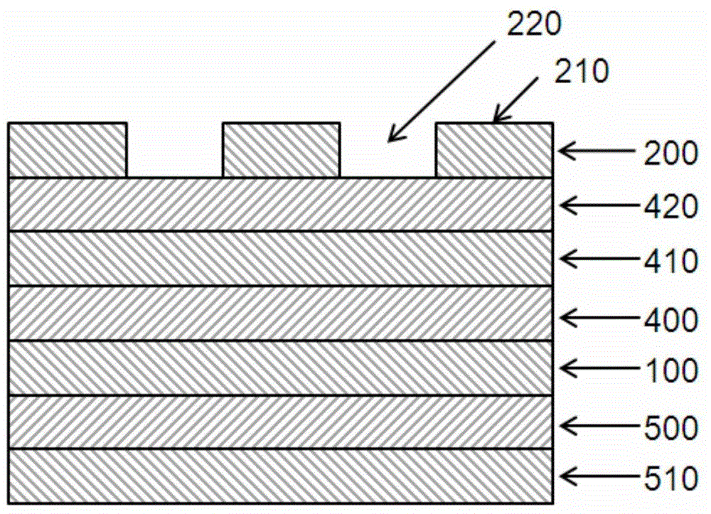
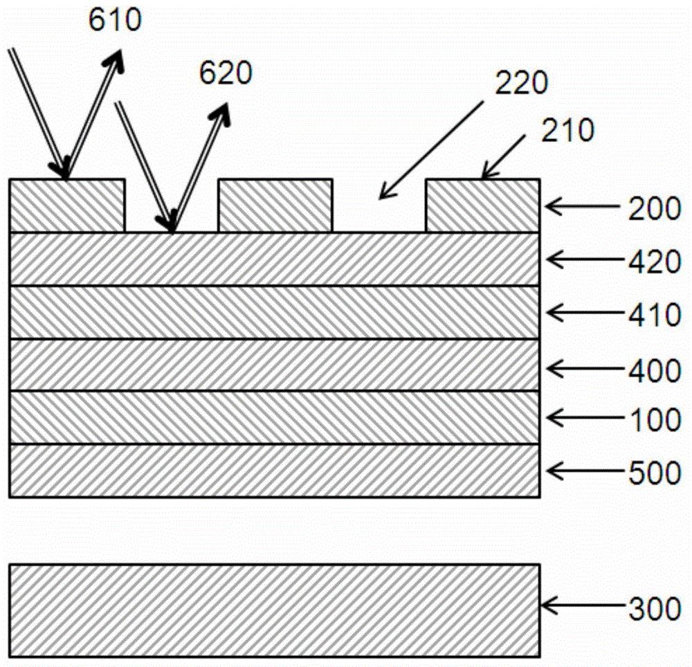
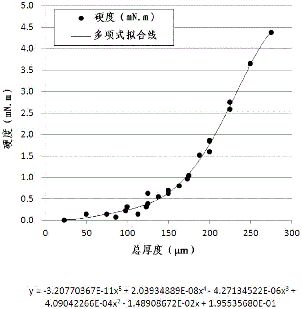
[0191] The transparent conductive optical sheet was produced in the same steps as in Example 1, and the total thickness was adjusted to 23-125 μm.

[0192] Moreover, a hardness-enhancing film having a base film layer with a thickness of 38 to 125 μm and an adhesive functional layer with a thickness of 20 to 50 μm formed on one of its surfaces was prepared. At this time, the base film layer was made of a PET transparent substrate. material, the adhesive functional layer includes 100 parts by weight of acrylic polymer resin and 0.001-10 parts by weight of isocyanate crosslinking agent (polyfunctional isocyanate compound).

[0193] Then, a transparent conductive optical sheet having a hardness-improving film is manufactured by pasting the adhesive functional layer of the hardness-improving film on the transparent base layer of the optical sheet.

[0194] However, for comparison, some tr...


PUM

PropertyMeasurementUnit
Thicknessaaaaaaaaaa
Thicknessaaaaaaaaaa
Thicknessaaaaaaaaaa

Abstract

The invention relates to a transparent conductive optical sheet having high invisibility of a pattern. The transparent conductive optical sheet comprises an ITO layer via etching of a pattern. Via a thin film drying effects of a reflectivity matching layer of the optical sheet, difference between the reflectivity and reflecting color between a non-etching part and an etching part of the ITO layer is corrected, and a user is allowed to fail to recognize the non-etching part and the etching part visually, so definition for display of a display panel on a lower part will not be reduced. In particular, when thickness of the ITO layer is changed for adjustment of surface resistance, even if the reflectivity and thickness of a transparent base layer or the reflectivity matching layer are changed, the thin film drying effects can be well maintained. Thus, the optical sheet can be suitable for touch display panel field of display panels of all kinds of electrical devices.

Description

technical field [0001] The invention relates to a transparent conductive optical sheet containing indium tin oxide (ITO). More specifically, it relates to a transparent conductive optical sheet including an ITO layer formed by etching a pattern or the like for a touch screen panel or the like. Background technique [0002] In recent years, touch screen panels (touch screen panels, TSPs) are widely used in display parts such as mobile phones, tablet devices, and monitors. The core material of this TSP mainly uses an optical sheet including ITO, a transparent conductive material. [0003] When an optical sheet including ITO is used for a touch screen panel or the like, a part of the ITO layer is generally etched to form a sensing pattern. However, ITO has inherent dispersion characteristics in which the refractive index increases when moving from the visible light band (380 to 780 nm) to the short wavelength direction. In particular, light reflected on the ITO layer is refle...

Claims


Application Information

Patent Timeline
IPC IPC(8): G06F3/041G02B1/16
CPCG06F3/041
Inventor 禹硕钟朴俊纪片升勇李庚男高银圭
Owner 爱思开迈克沃解决方案有限公司
Why Eureka
Try Eureka