Probe card

a technology of probe card and probe, which is applied in the field of probe card, can solve the problems of creating ground noise in the probe card, incorrectly testing the normally operative chips as defective chips, and causing errors in the test, so as to reduce the ground noise

Inactive Publication Date: 2005-06-21
SAMSUNG ELECTRONICS CO LTD
View PDF5 Cites 62 Cited by
  • Summary
  • Abstract
  • Description
  • Claims
  • Application Information

AI Technical Summary

Benefits of technology

[0019]It is an object of the present invention to provide a probe card which exhibits a reduction in ground noise.

Problems solved by technology

However, as explained below, the conventional probe card suffers from ground noise which can result in erroneous test results.
The common electrical connection of ground signals PG, CG1 to CGm and G1 to Gn within the probe card of the conventional test apparatus can cause problems when the ground signals are applied to the ground pads of the chips of the wafer 18.
More specifically, when multiple chips are simultaneously tested at a high operating speed, the multiple test signals thereof having the common ground can create ground noise in the probe card.
This ground noise can in turn result in normally operative chips being incorrectly tested as defective chips.

Method used


Image

  • Probe card
  • Probe card
  • Probe card

Examples


Embodiment Construction

[0028]Reference will now be made in detail to preferred embodiments of the present invention, an example of which is illustrated in the accompanying drawings.

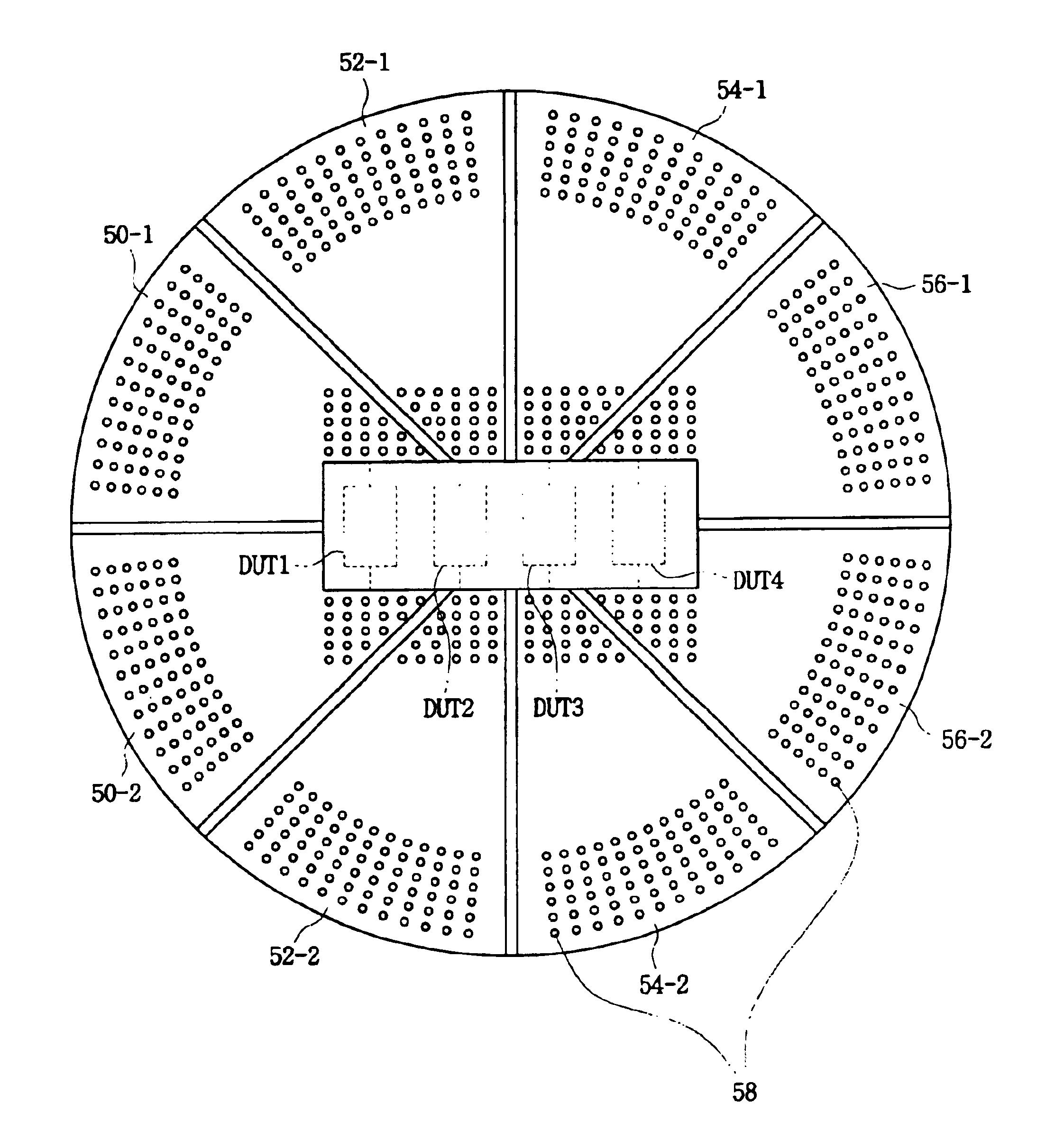
[0029]FIG. 4 shows a ground printed circuit board of a probe card according to an embodiment of the present invention. The probe card of this embodiment is configured as illustrated in FIGS. 1 and 2, except that it includes ground printed circuit board of FIG. 4 rather than that of FIG. 3. The dashed lines of FIG. 4 denote regions of chips DUT1, DUT2, DUT3 and DUT4 being tested.

[0030]In FIG. 4, the symbol “o” denotes signal application holes, reference numerals 50-1, 52-1, 54-1, and 56-1 denote conductive regions containing holes for applying the ground signals PG, CG1 to CGm of the respective chips DUT1 to DUT4, and reference numerals 50-2, 52-2, 54-2, and 56-2 denote conductive regions containing holes for applying the ground signals G1 to Gn of the respective chips DUT1 to DUT4. Also, the holes “o” include application holes ...


PUM


Abstract

A probe card is provided which includes a plurality of stacked signal printed circuit boards for transmitting signals, and a plurality of ground printed circuit boards respectively interposed between the signal printed circuit boards. To reduce ground noise, each of the ground printed circuit boards includes a plurality of conductive ground regions which are insulated from each other.

Description

BACKGROUND OF THE INVENTION[0001]1. Field of the Invention[0002]The present invention relates to a probe card, and more particularly, the present invention relates to a probe card used to test electrical characteristics of chips on a semiconductor wafer.[0003]A claim of priority under 35 U.S.C. § 119 it made to Korean Patent Application 2003-3514 filed on Jan. 18, 2003, the entire contents of which are hereby incorporated by reference.[0004]2. Description of the Related Art[0005]A semiconductor test apparatus, which is used to test electrical characteristics of chips manufactured on a wafer, typically includes a tester, a performance board, a probe card, a chuck, and a prober.[0006]The probe card of the semiconductor test apparatus is made up of a stack of alternately arranged signal printed circuit boards and ground printed circuit boards. The signal printed circuit boards are for applying power supply signals, command and address signals, and data signals, and the ground printed c...

Claims


Application Information

Patent Timeline
Patent Type & Authority Patents(United States)
IPC IPC(8): G01R1/073H01L21/66
CPCG01R1/07342H01L22/00
Inventor JI, JOON-SUHWANG, IN-SEOKLEE, DOO-SEONKIM, BYOUNG-JOORO, YOUNG-KYOLEE, HO-YEOL
Owner SAMSUNG ELECTRONICS CO LTD
Why Eureka
Try Eureka