

Semiconductor package having flex circuit with external contacts
a technology of flex circuits and semiconductors, applied in the field of semiconductor packaging, can solve the problems of weakening or pulling apart bonds, difficult fabrication of dense arrays of external contacts,
- Summary
- Abstract
- Description
- Claims
- Application Information
AI Technical Summary
Benefits of technology
Problems solved by technology
Method used
Image

Examples
Embodiment Construction
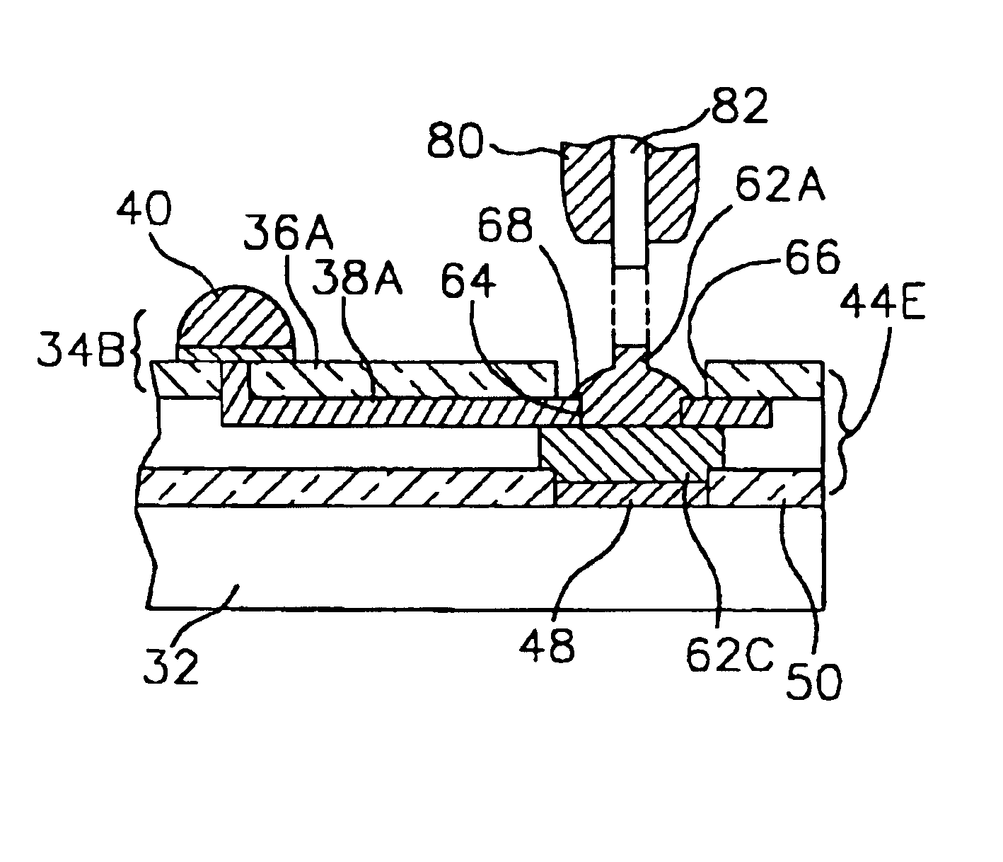
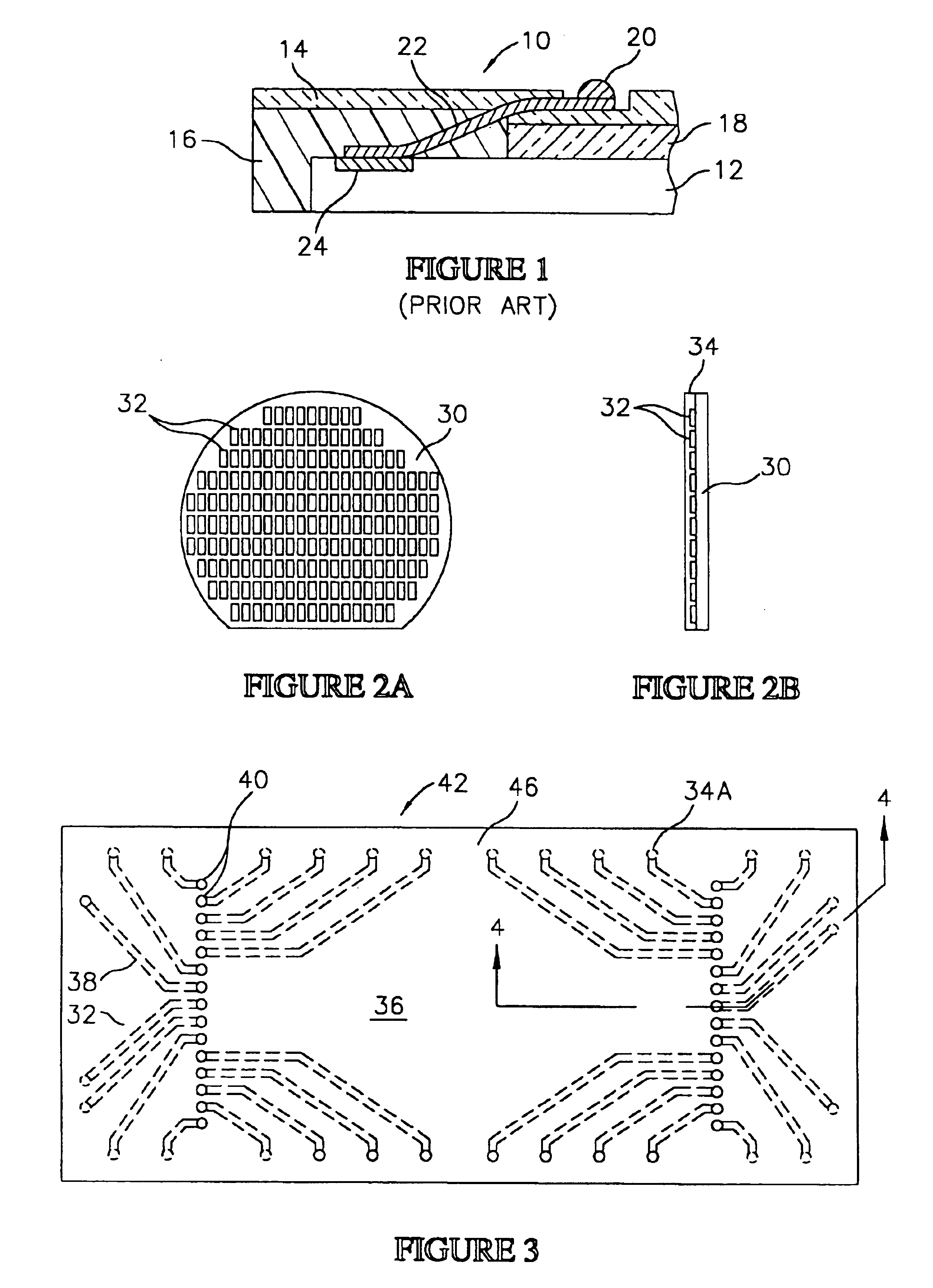
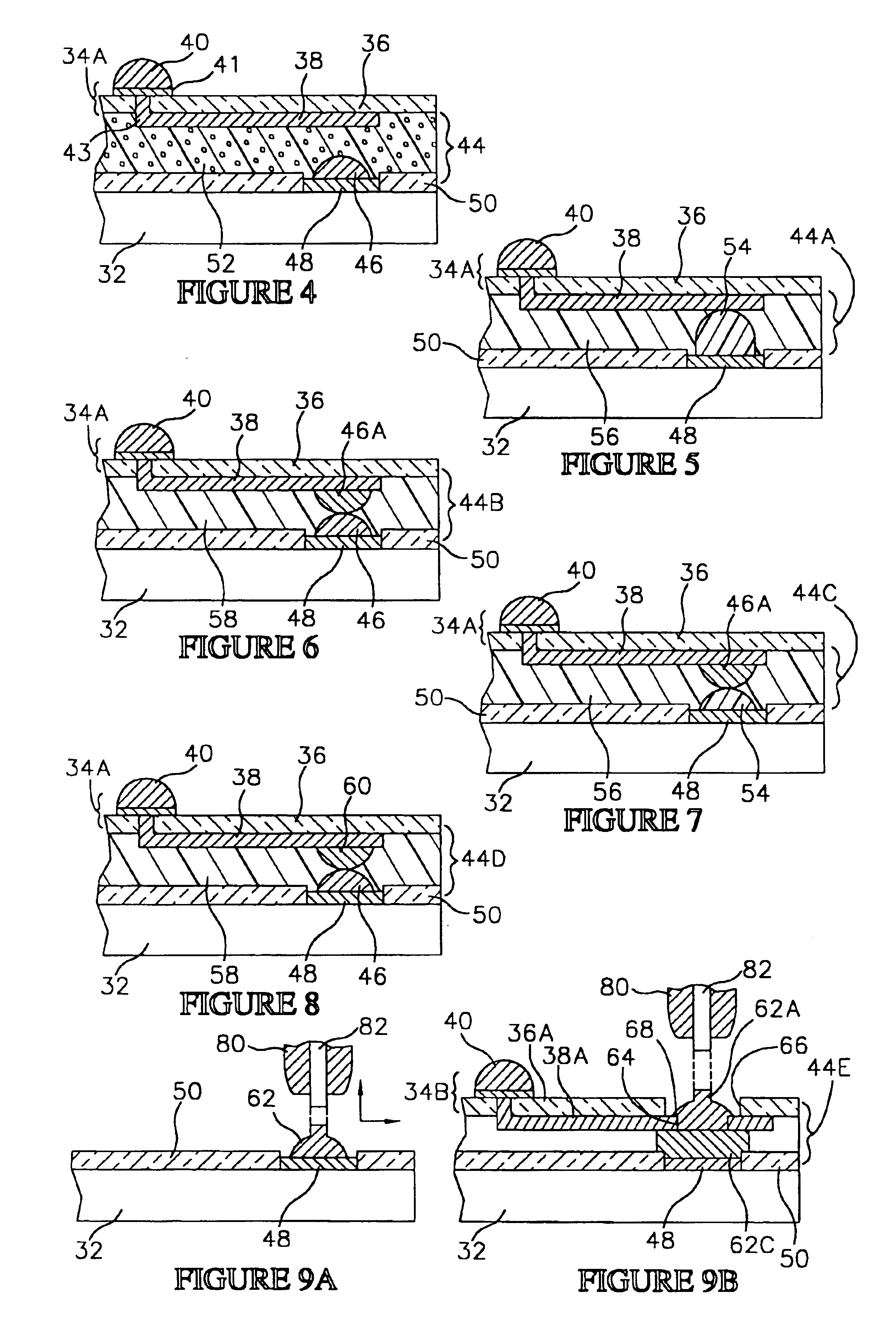
[0038]Referring to FIGS. 2A-2B, steps in a wafer level process for fabricating chip scale semiconductor packages in accordance with the invention are illustrated. Initially, as shown in FIG. 2A, a semiconductor wafer 30 can be provided. The wafer 30 includes multiple semiconductor dice 32. Each die 32 has a desired size and peripheral shape (e.g., rectangular, square). In addition, each die 32 includes integrated circuits in a desired configuration. Still further, each die 32 includes die contacts 48 (FIG. 4) in electrical communication with the integrated circuits. The die contacts 48 (FIG. 4) can be conventional thin film aluminum bond pads formed on the face of the die.
[0039]As shown in FIG. 2B, a sheet of flex circuit 34 can be bonded to a face (circuit side) of the wafer 30. The flex circuit 34 comprises a multi layered sheet of material similar to TAB tape, such as “ASMAT” manufactured by Nitto Denko. The flex circuit 34 can be formed separately, and then bonded to the wafer 3...
PUM
 Abstract
Description
Claims
Application Information