Non-volatile memory with functional capability of simultaneous modification of the content and burst mode read or page mode read

a non-volatile memory and content technology, applied in the field of semiconductor memory, can solve the problem of not being able to benefit from the possibility of reducing the access time offered

Inactive Publication Date: 2005-06-28
MICRON TECH INC
View PDF7 Cites 36 Cited by
  • Summary
  • Abstract
  • Description
  • Claims
  • Application Information

AI Technical Summary

Benefits of technology

[0006]An embodiment of the present invention provides a memory that has the functional capability of simultaneous modification of its own content and burst mode read or page mode read. The memory includes two memory banks that are substantially independent of each other; a first control circuit that controls operations of electrical alteration of content of the memory and permits the selective execution of an operation of electrical alteration of the content of a first one of the two memory banks; and a second control circuit that permit

Problems solved by technology

The read is however a standard type read, therefore does not benefit from the possibilities of

Method used


Image

  • Non-volatile memory with functional capability of simultaneous modification of the content and burst mode read or page mode read
  • Non-volatile memory with functional capability of simultaneous modification of the content and burst mode read or page mode read
  • Non-volatile memory with functional capability of simultaneous modification of the content and burst mode read or page mode read

Examples


Embodiment Construction

[0007]The features and advantages of the present invention will become clear from the following detailed description of one of its embodiments, illustrated by way of non-limiting example in the appended drawings, in which:

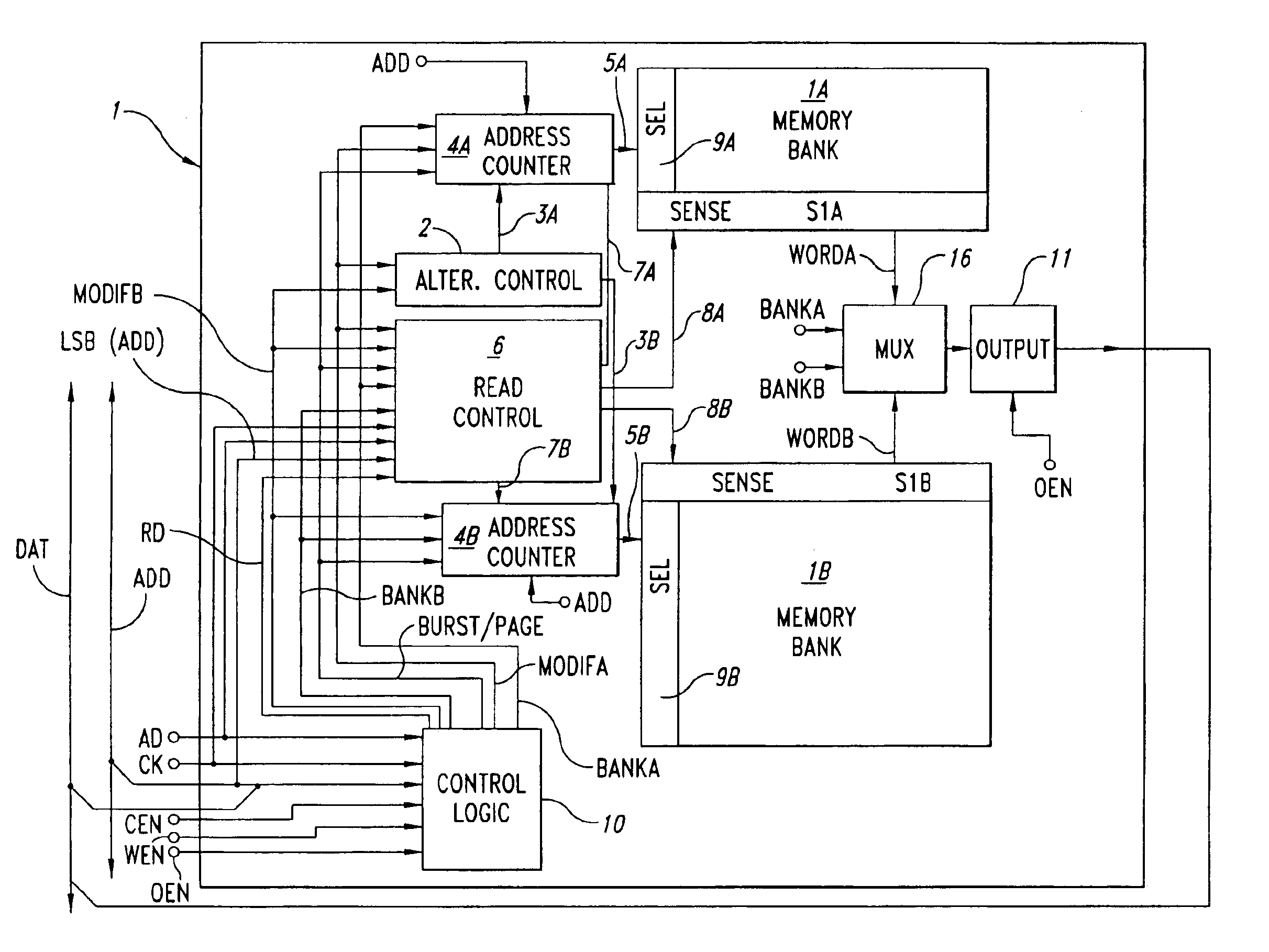
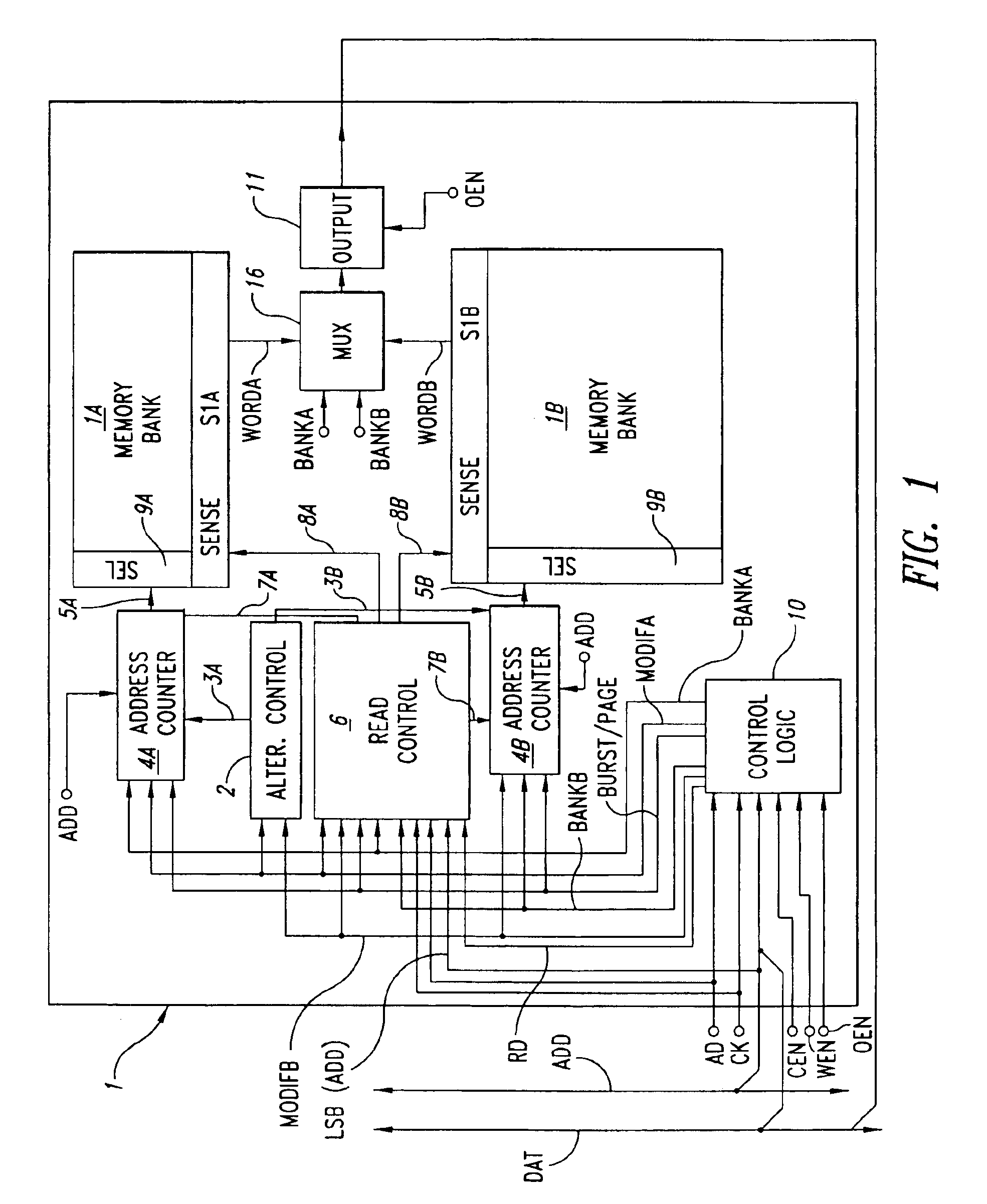
[0008]FIG. 1 shows diagrammatically, at the level of the principal functional blocks, a memory according to the present invention;

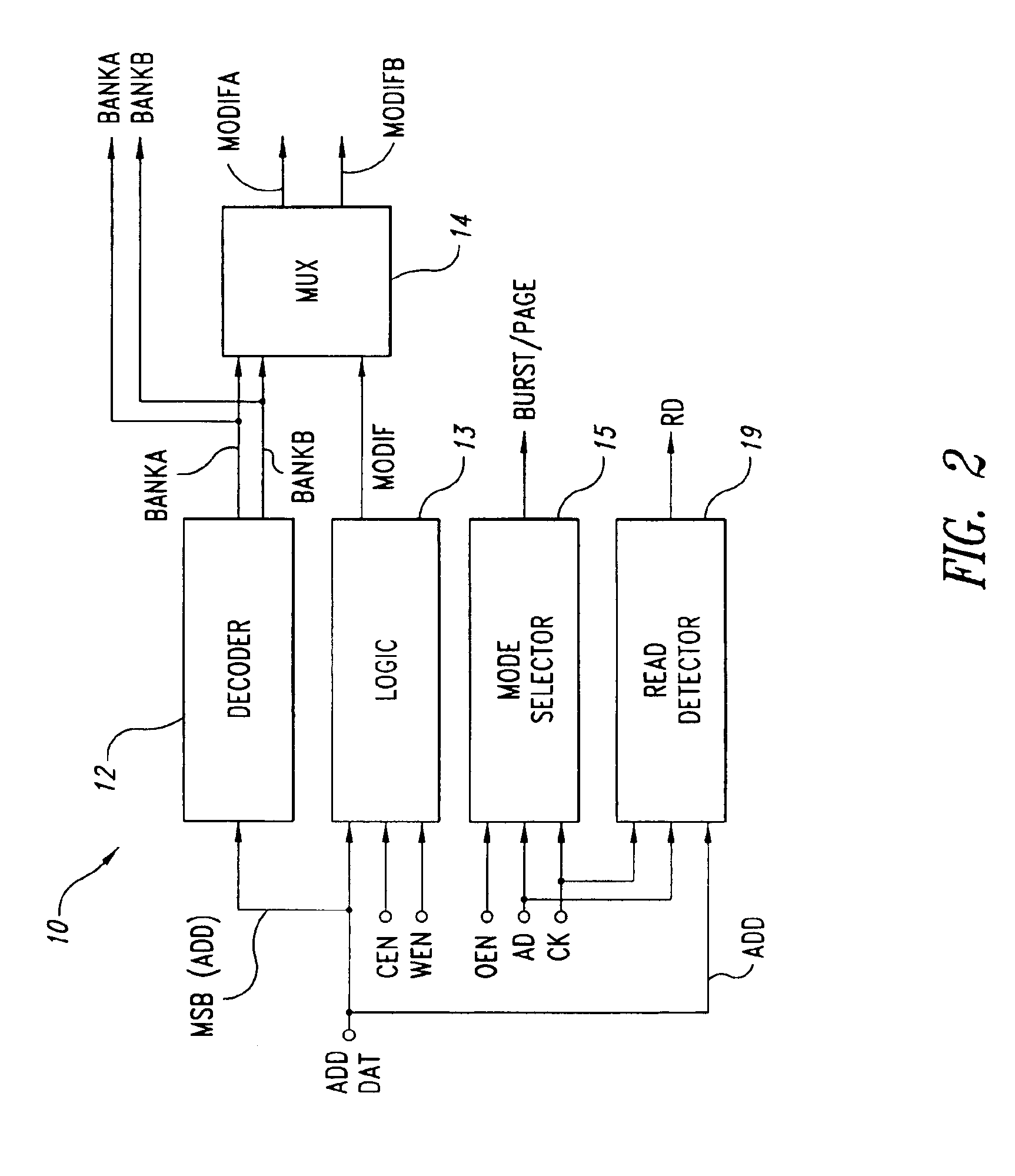
[0009]FIG. 2 is a block diagram of a logic circuit for controlling the memory in FIG. 1;

[0010]FIG. 3 is a more detailed block diagram of part of the memory in FIG. 1; and

[0011]FIGS. 4 and 5 are simplified diagrammatic views, in terms of logic gates, of the operation of a circuit for controlling the operations of burst mode read or page mode read of the memory in FIG. 1.

DETAILED DESCRIPTION OF THE INVENTION

[0012]With reference to the drawings, a non-volatile memory 1 with electrically alterable content, for example an EPROM, or EEPROM, or Flash EEPROM memory, comprises two independent memory banks 1A, 1B, of either the same size or differ...


PUM


Abstract

An electrically alterable semiconductor memory comprises at least two substantially independent memory banks, and a first control circuit for controlling operations of electrical alteration of the content of the memory. The first control circuit permits the selective execution of an operation of electrical alteration of the content of one of the at least two memory banks. The memory also comprises second control circuit that permits, simultaneously with said operation of electrical alteration of the content of one of the at least two memory banks, a burst mode, page mode, or standard read operation for reading the content of the other memory bank.

Description

TECHNICAL FIELD[0001]The present invention relates to the field of semiconductor memories, in particular non-volatile memories, and still more particularly memories the content of which is electrically alterable (programmable or both programmable and erasable), such as EPROMs, EEPROMs and Flash EEPROMs.BACKGROUND OF THE INVENTION[0002]A normal read operation (hereinafter, standard read) in a memory provides for supplying to the memory an address which identifies a corresponding location of the memory. After a specific time interval has elapsed, termed access time, the datum stored in said location is available at the output of the memory.[0003]Memories are known in which, besides the standard reading operation, it is possible to carry out a page mode read operation which, in the case where only the less significant bits of the address supplied at the input of the memory vary, makes it possible to obtain valid data at the output of the memory in a shorter time than the standard acces...

Claims


Application Information

Patent Timeline
IPC IPC(8): G11C16/10G11C16/26
CPCG11C16/10G11C16/26
Inventor BEDARIDA, LORENZOGERACI, ANTONINOSALI, MAUROBARTOLI, SIMONE
Owner MICRON TECH INC
Why Eureka
Try Eureka