Process for imagewise opening and filling color display components and color displays manufactured thereof

Inactive Publication Date: 2005-07-05
E INK CALIFORNIA
View PDF25 Cites 78 Cited by
  • Summary
  • Abstract
  • Description
  • Claims
  • Application Information

AI Technical Summary

Benefits of technology

[0022]The resulting simple and efficient manufacturing processes disclosed in this invention provide high quality, high resolution multi-color displays with significantly lower processing costs, less defects, higher yields, and no crosstalk among neighbori

Problems solved by technology

However, the filling and sealing processes of electrophoretic fluids in these cells are of very low throughput and high cost.
However, where the manufacture of high contrast ratio color displays requires the use of microcups that are structurally wide and deep, resulting in relatively thin partitions between the microcups, defects in the finished displays are often observed.
These defects may be attributed to,

Method used


Image

  • Process for imagewise opening and filling color display components and color displays manufactured thereof
  • Process for imagewise opening and filling color display components and color displays manufactured thereof
  • Process for imagewise opening and filling color display components and color displays manufactured thereof

Examples


example 1

Microcup Formulation

[0053]35 parts by weight of Ebecryl 600 (UCB), 40 parts of SR-399 (Sartomer), 10 parts of Ebecryl 4827 (UCB), 7 parts of Ebecryl 1360 (UCB), 8 parts of HDDA (UCB), 0.05 parts of Irgacure 369 (Ciba Specialty Chemicals), and 0.01 parts of isopropyl thioxanthone (ITX, Aldrich) were mixed homogeneously and used for micro-embossing.

example 2

Preparation of Microcup Array

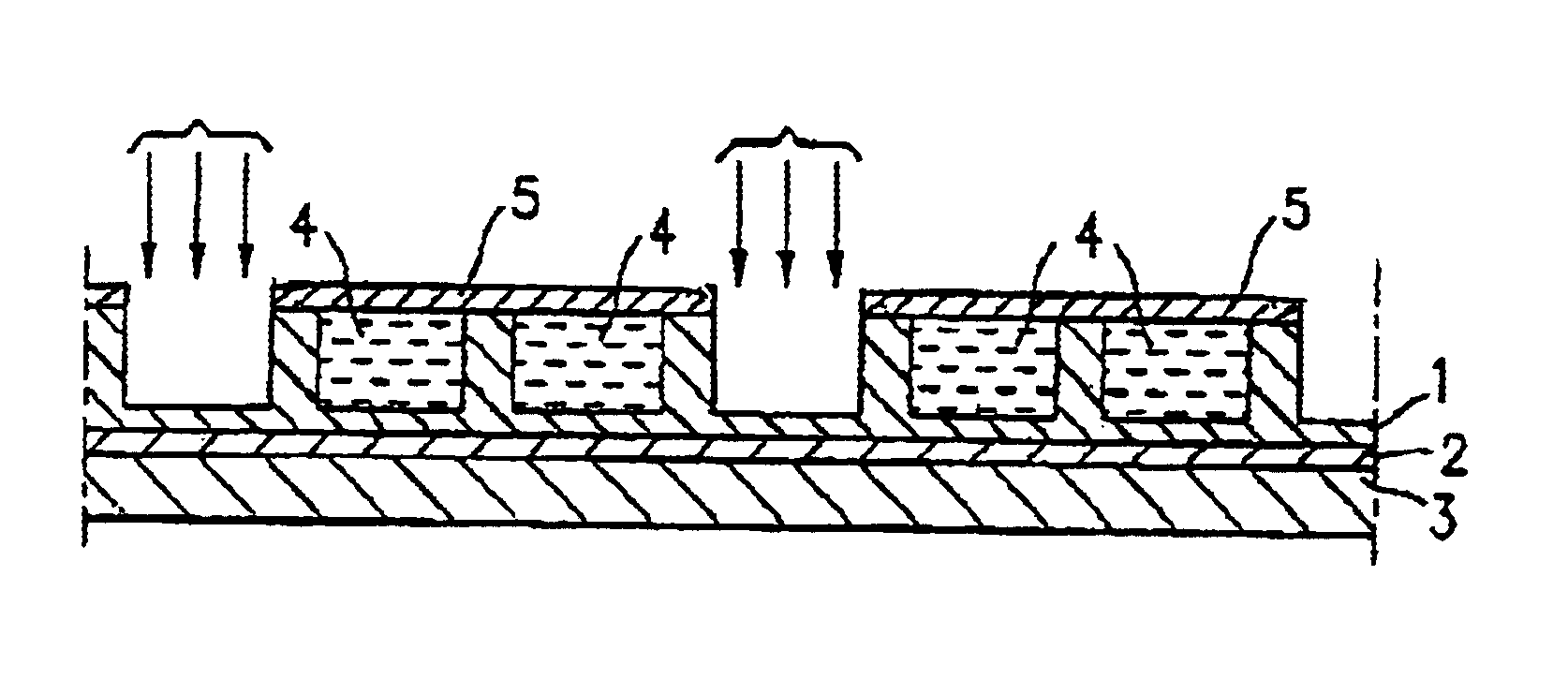
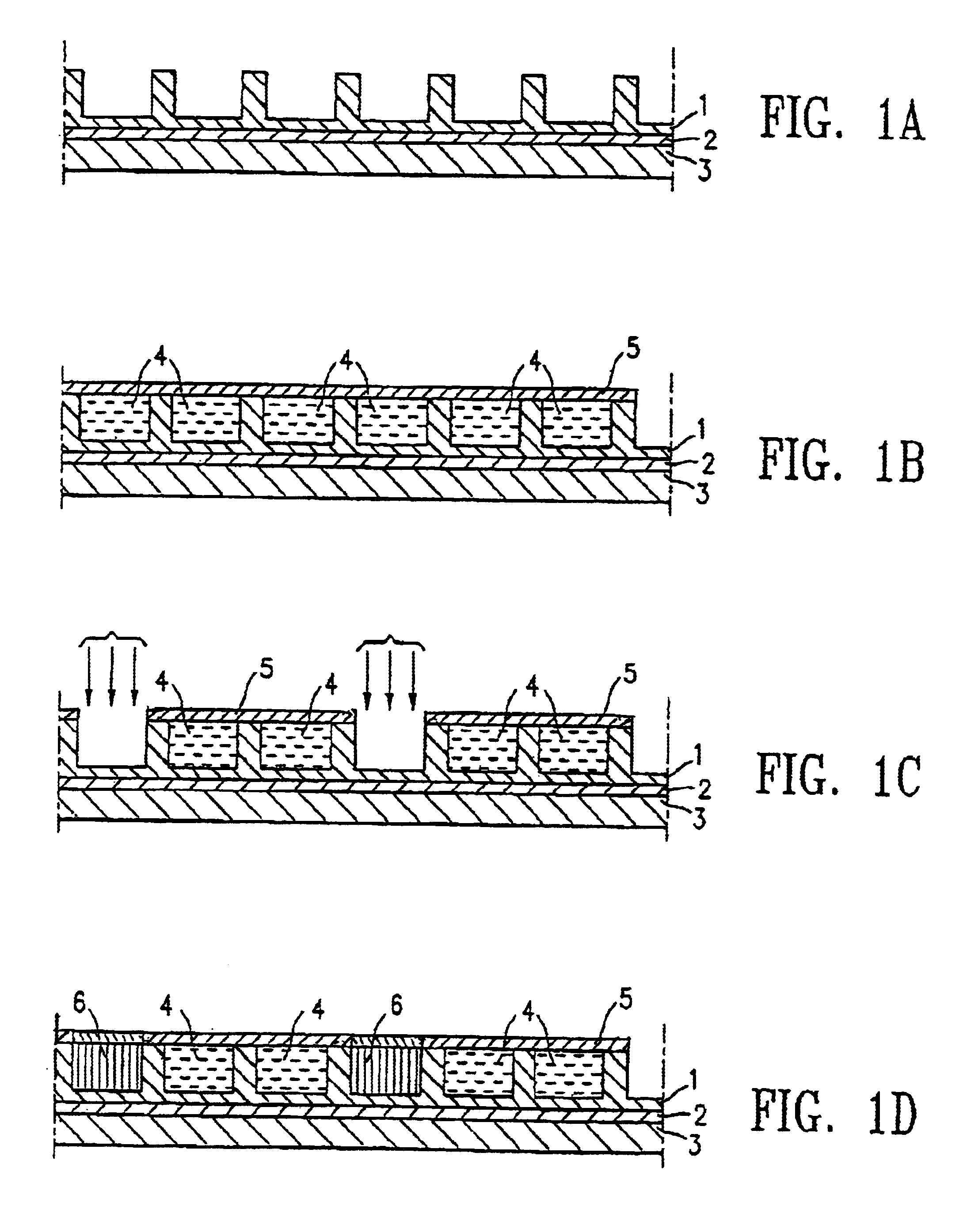
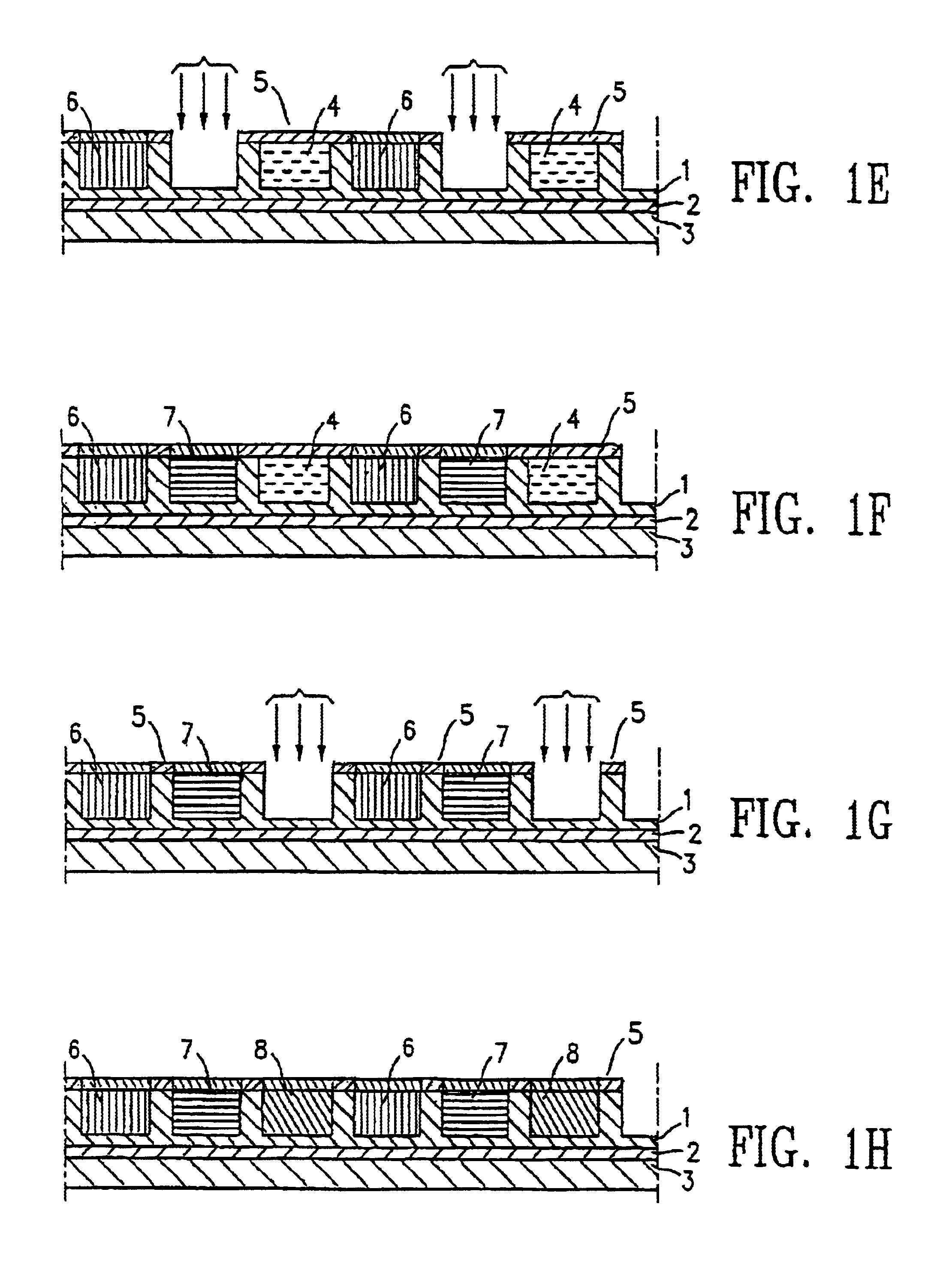
[0054]A primer solution comprising of 5 parts of Ebecryl 830, 2.6 parts of SR-399 (Sartomer), 1.8 parts of Ebecry 1701, 1 part of PMMA (Mw=350,000, Aldrich), 0.5 parts of Irgacure 500, and 40 parts of methyl ethyl ketone (MEK) was coated onto a 2 mu 60 ohm / sq. ITO / PET film (Sheldahi Inc., MN) using a #3 Myrad bar, dried, and UV cured by using the Zeta 7410 (5 w / cm2, Loctite) exposure unit for 15 minutes in air. The microcup formulation prepared in Example 1 was coated onto the treated ITO / PET film with a targeted thickness of about 50 μm, embossed with a Ni—Co male mold having a 60 (width) μm×60 (length) μm repetitive protrusion pattern with 10 μm wide partition lines and UV cured from the PET side for 20 seconds, removed from the mold with a 2″ peeling bar at a speed of about 4-5 ft / min. Well-defined microcups with depth ranging from 10 to 50 μm were prepared by using male molds having corresponding protrusion heights.

example 3

Comparative Example: Microcup Array Laminated with Novolac Photoresist

[0055]3 Gm / m2 (dried) of the positively working photoresist SJR-5740 (Shipley, Mass.) was coated on a removable clear support PET-4851 (Saint-Gobain, Mass.) with a Myrad bar. Onto the photoresist, 3 gm / m2 (dried) of an alkali-developable adhesive composition comprising of 9 parts of Nacor 72-8685 (50% solid, National Starch) and 91 parts of 20% aqueous solution of Carboset 515 (BF Goodrich) was then coated with a Myrad bar. The three layer adhesive / resist / support was then laminated at 40° C. onto a 10 microns deep, empty microcup array prepared according to Example 2. The PET support was removed, and the photoresist laminated microcup array was imagewise exposed through a photomask using the Zeta 7410 (5 w / cm2, Loctite) exposure unit for about 1 minute and then developed by Developer-453 (Shipley) for 2 minutes. Deterioration of resist integrity in the non-exposed regions such as pinholes and delamination of resis...


PUM


Abstract

This invention relates to the field of electrophoretic displays. In particular, it relates to imagewise opening, filling, and sealing multicolor display components and the manufacture of multicolor displays.

Description

[0001]This application is a continuation of U.S. application Ser. No. 10 / 284,586, filed Oct. 30, 2002, which is a continuation-in-parts of U.S. application Ser. No. 09 / 879,408, filed Jun. 11, 2001, now U.S. Pat. No. 6,545,797, the contents of which are incorporated herein by reference in their entirety.FIELD OF INVENTION[0002]This invention relates to the field of electrophoretic displays. In particular, it relates to imagewise opening and filling multicolor display components and the manufacture of multicolor displays.BACKGROUND OF THE INVENTION[0003]Electrophoretic displays (EPDs) are known non-emissive displays suitable for use in the display of digital, alphanumeric, analog or graphical information. An EPD system typically comprises a suspension of pigment particles in a dielectric liquid held between two electrodes, at least one of which is transparent. Applied potential across the electrodes causes the charged particles to migrate to one or the other electrode. Where the suspe...

Claims


Application Information

Patent Timeline
IPC IPC(8): G02F1/01G02F1/13G02F1/1333G02F1/1341G02F1/167G02F1/1347
CPCG02F1/133377G02F1/1341G02F1/167G02F1/1347G02F2001/1672G02F1/1681
Inventor CHEN, XIANHAIZANG, HONGMEIWU, ZARNG-ARH GEORGELIANG, RONG-CHANG
Owner E INK CALIFORNIA
Why Eureka
Try Eureka