Tray for electronic components

a technology for electronic components and trays, which is applied in the direction of transportation and packaging, electrical apparatus construction details, and casings/cabinets/drawers of electrical apparatus, etc., can solve the problems of small size and requirement of electronic components, and achieve the effect of preventing damag

Inactive Publication Date: 2005-07-05
ONO HIROKAZU +1
View PDF4 Cites 14 Cited by
  • Summary
  • Abstract
  • Description
  • Claims
  • Application Information

AI Technical Summary

Benefits of technology

[0022]The present invention solves the above mentioned technical problems and its object is t...

Problems solved by technology

Such electronic components are known to be small-sized...

Method used


Image

  • Tray for electronic components
  • Tray for electronic components
  • Tray for electronic components

Examples


Embodiment Construction

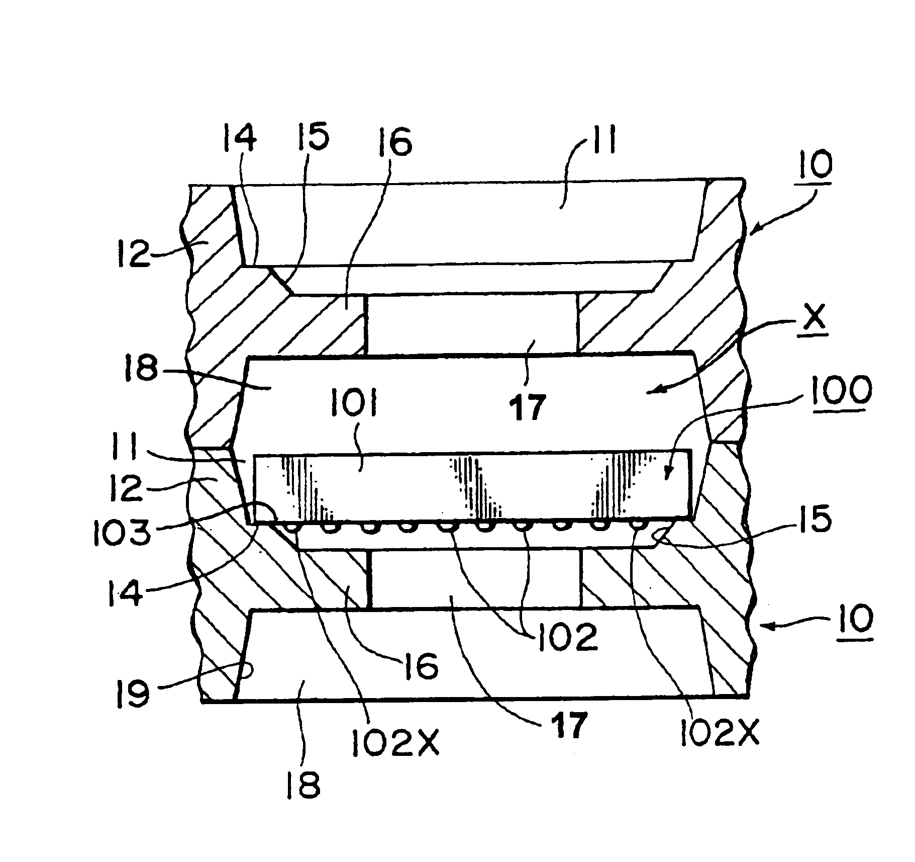
[0036]Hereinafter, it is to be noted before the explanation of the embodiments of the tray according to the present invention that detailed explanation of the members bearing similar numerals as those of the prior art explained with reference to FIG. 8 is omitted

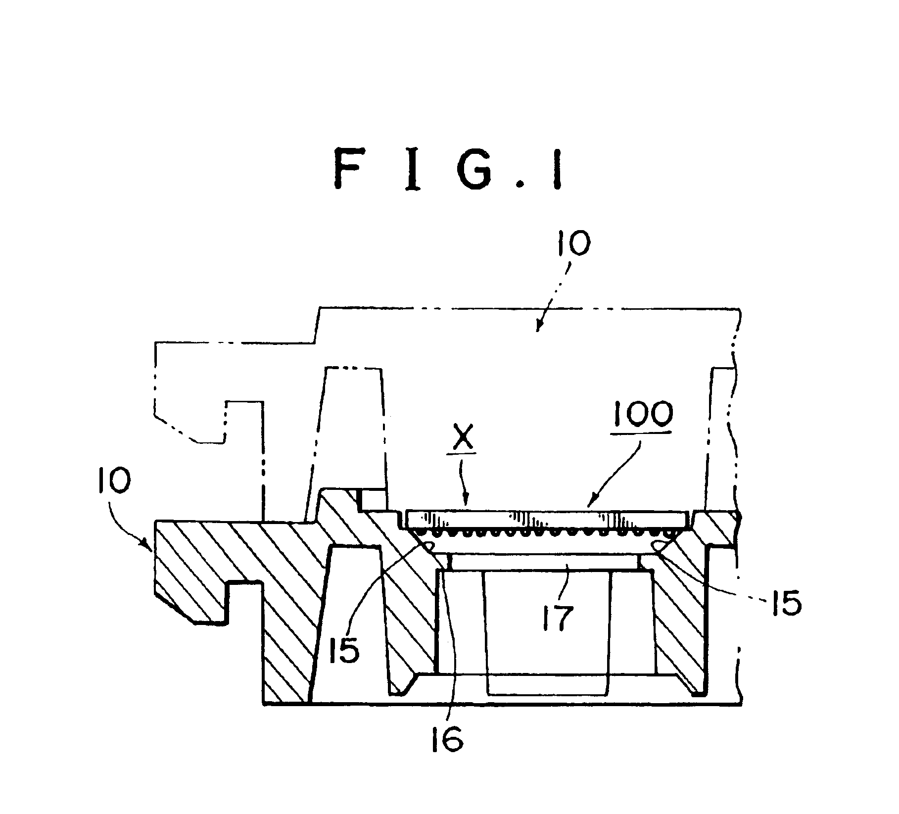
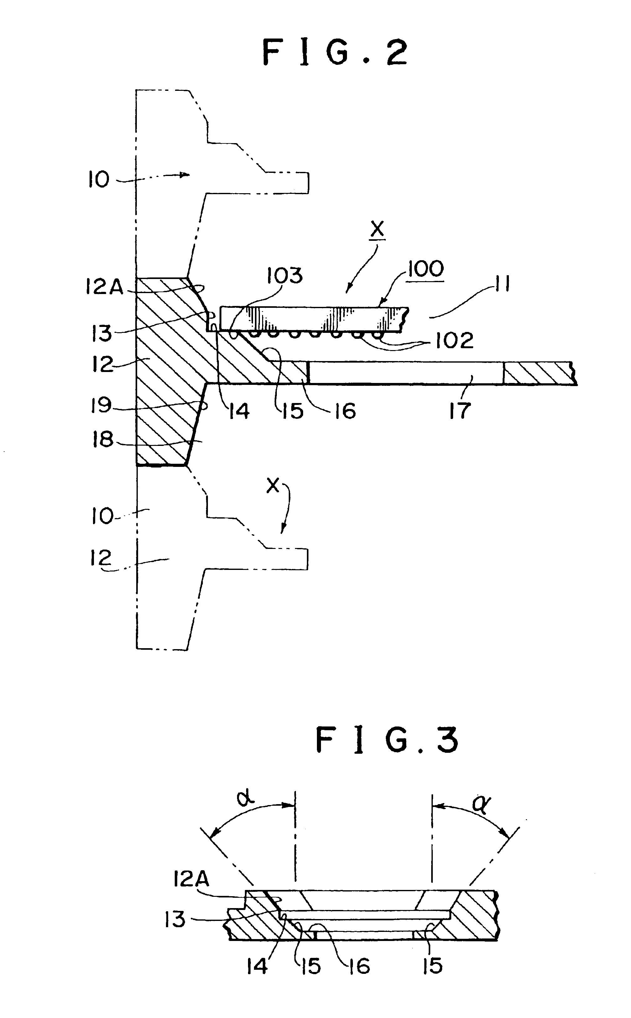
[0037]First, FIG. 1 shows part of the tray for the electronic components (hereinafter referred to as a “tray”) is shown in cross section, wherein the electronic component 100 is substantially a square board 101 having a side length of 4.45 mm in plan view, a thickness of 0.63 mm, and a width of 0.34 mm at the peripheral portion 103 thereof formed around the contacts 102, all of said dimensions being similar to those of the prior art explained so far. The closed cavities to accommodate are formed in the laminated tray 10.

[0038]Further, the embodiment of the present invention will be explained with reference to the attached drawings including FIGS. 1 through 7. The numeral 10 denotes a tray in FIG. 1. A plurality of such trays...


PUM


Abstract

A tray for accommodating electronic components with edge portions and contacts includes a main portion for forming the tray, and a plurality of accommodation cavities formed in the tray for accommodating a plurality of electronic components therein. Each accommodation cavity includes partition walls for surrounding the electronic components, support steps extending horizontally inwardly from lower ends of the partition walls to form a first space therein and to support the edge portions of the electronic component, and descending walls extending downwardly from the support steps to define the first space. Each partition wall has a lower portion with a first inclination for a mold removing operation, and each descending wall has a second inclination greater than that of the first inclination to be able to contact and support an edge of the electronic component when falling from the edge portion.

Description

BACKGROUND OF THE INVENTION[0001]The present invention relates to a tray for electronic components and more particularly to an electronic component tray used for conveying or inspecting electronic components known as semiconductor devices of a bowl grid array (BGA) type.[0002]Electronic components of semiconductor devices known as semiconductor chips are composed of integrated circuits such as wafers. A typical example thereof includes an electronic component known as a BGA type semiconductor device. Such electronic components are known to be small-sized and required to be manufactured in a clean air environment.[0003]Further, trays for electronic components are being used not only for conveying electronic components in the manufacturing process but also for efficiently handling electronic components for the purposes of inspection or prevention of electrostatic discharge damage thereof.[0004]Conventionally used trays for electronic components include those as shown in FIG. 10, which...

Claims


Application Information

Patent Timeline
IPC IPC(8): H01L21/673H01L21/67H05K13/00
CPCH01L21/67333H05K13/0084H01L2221/68313H01L21/68
Inventor ONO, HIROKAZUTESHIMA, KUNIHIRO
Owner ONO HIROKAZU
Why Eureka
Try Eureka