IC with wait state registers

Inactive Publication Date: 2005-07-12
TEXAS INSTR INC
View PDF7 Cites 12 Cited by
  • Summary
  • Abstract
  • Description
  • Claims
  • Application Information

AI Technical Summary

Benefits of technology

[0012]Generally, another form of the invention is a data processing system including an analog-to-digital converter and an electronic processor connected to the analog-to-digital converter and having an electronic computation unit for executing operations and an accumulator having status conditions including A) carry, B) overflow and C) contents relative to a predetermined number wherein a particular one or more of the status conditions can occur in operation. An instruction register is operative to hold a conditi

Problems solved by technology

Such general-purpose microprocessors, while having good performance for a wide range of arithmetic and logical functions, are of course not specifically designed for or adapted to

Method used


Image

  • IC with wait state registers
  • IC with wait state registers
  • IC with wait state registers

Examples


Embodiment Construction

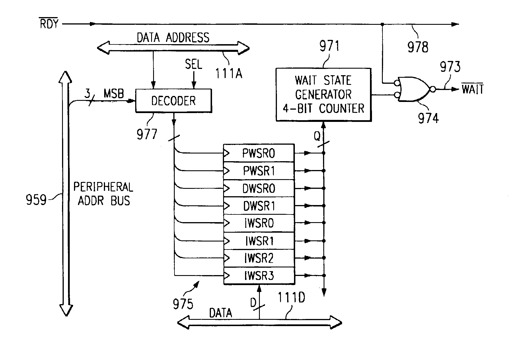
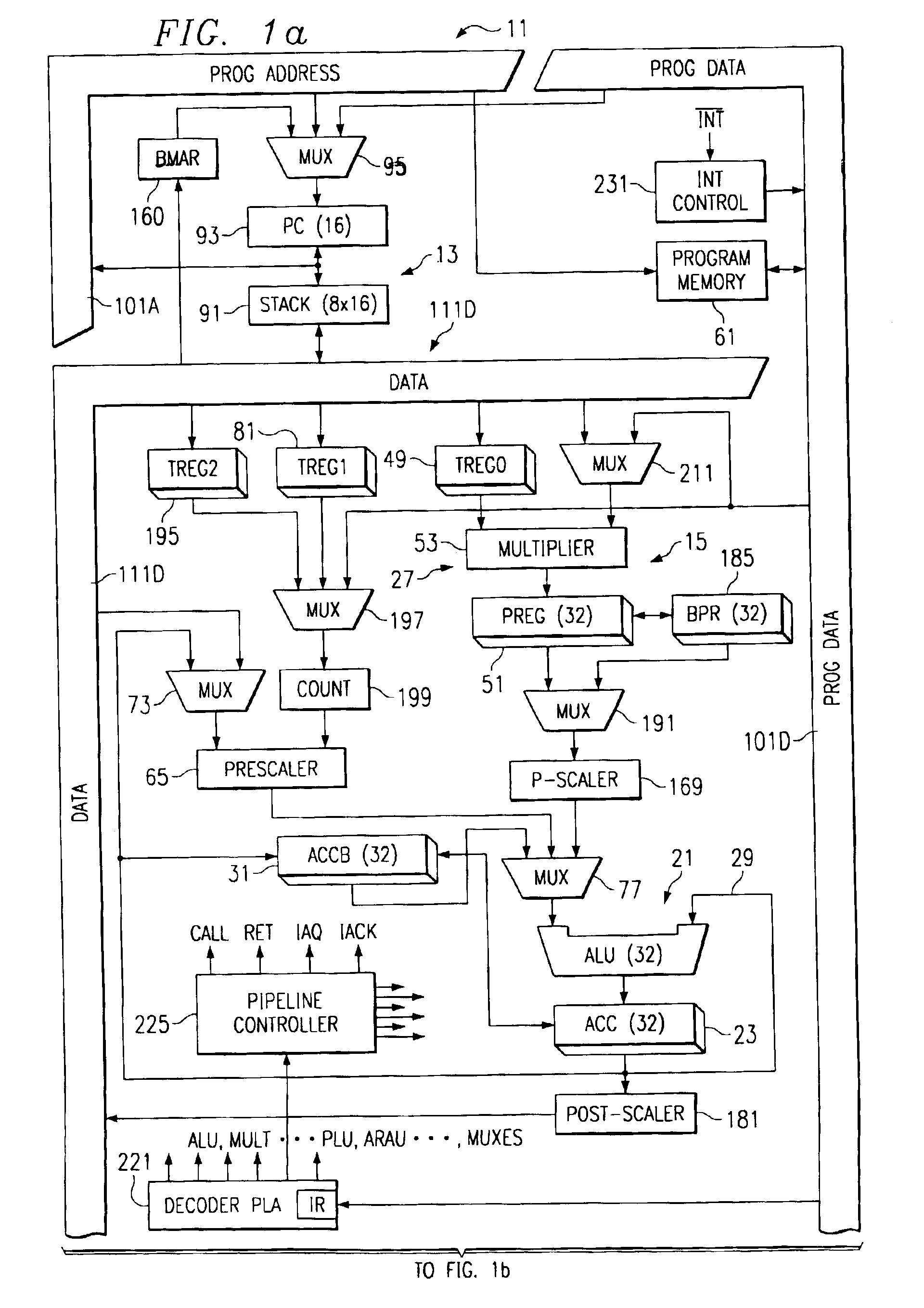
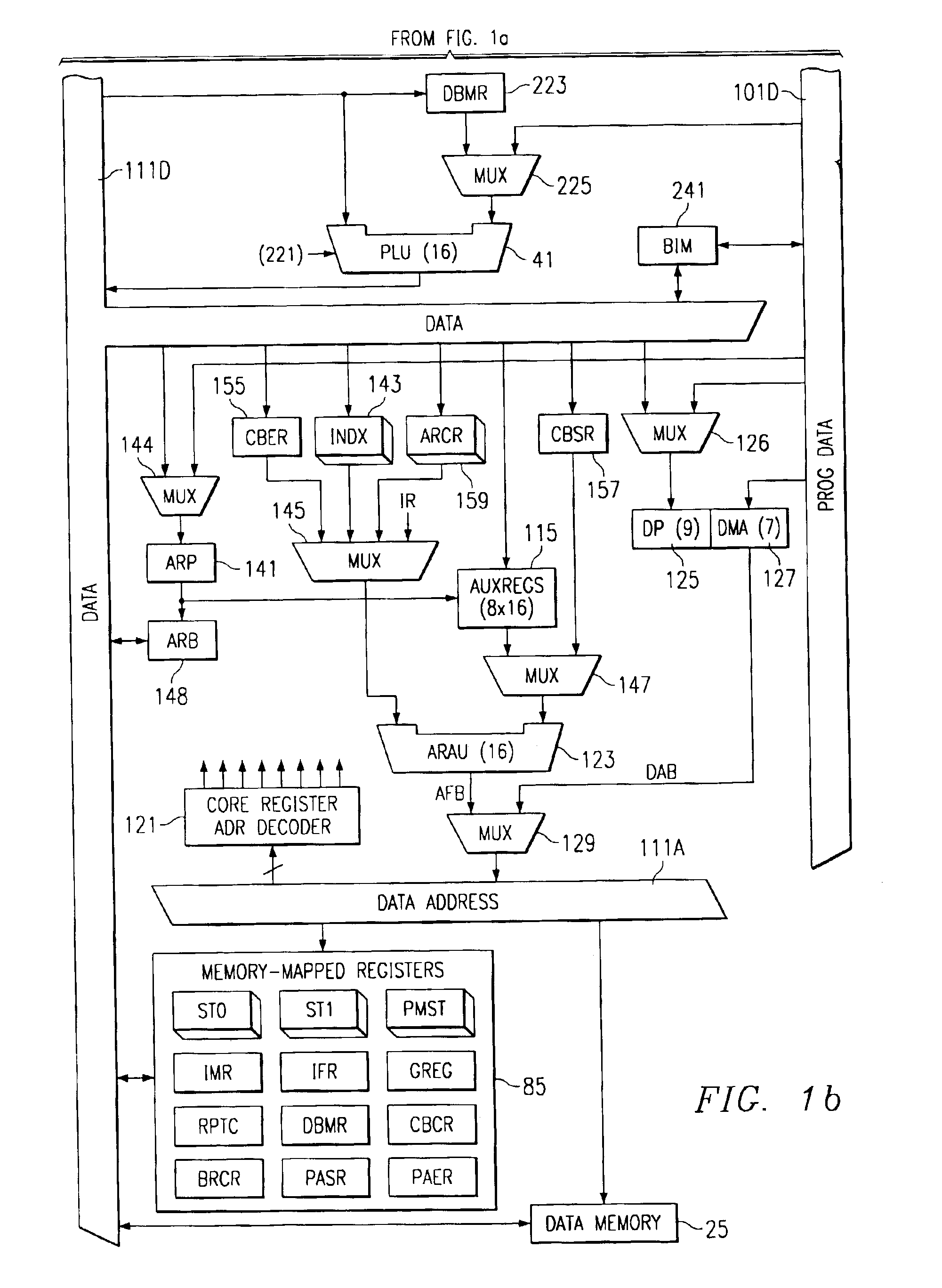
[0059]An architectural overview first describes a preferred embodiment digital signal processing device 11.

[0060]The preferred embodiment digital signal processing device 11 of FIGS. 1A and 1B implements a Harvard-type architecture that maximizes processing power by maintaining two separate memory bus structures, program and data, for full-speed execution. Instructions are included to provide data transfers between the two spaces.

[0061]The device 11 has a program addressing circuit 13 and an electronic computation circuit 15 comprising a processor. Computation circuit 15 performs two's-complement arithmetic using a 32 bit ALU 21 and accumulator 23. The ALU 21 is a general-purpose arithmetic logic unit that operates using 16-bit words taken from a data memory 25 of FIG. 1B or derived from immediate instructions or using the 32-bit result of a multiplier 27. In addition to executing arithmetic instructions, the ALU 21 can perform Boolean operations. The accumulator 23 stores the outpu...


PUM


Abstract

A data processing device is used with peripheral devices having addressees and differing communication response periods. The data processing device includes a digital processor adapted for selecting different ones of the peripheral devices by asserting addresses of each selected peripheral device. Addressable programmable registers hold wait state values representative of distinct numbers of wait states corresponding to different address ranges. Circuitry responsive to an asserted address to the peripheral devices asserted by the digital processor generates the number of wait states represented by the value held in one of the addressable programmable registers corresponding to the one of the address ranges in which the asserted address occurs, thereby accommodating the differing communication response periods of the peripheral devices.

Description

CROSS REFERENCE TO RELATED APPLICATIONS[0001]This patent is related to co-assigned U.S. Pat. Nos. 5,586,275; 5,072,418; 5,142,677; 5,155,812; 5,829,054; and 5,724,248, all filed contemporaneously herewith and incorporated herein by reference.[0002]This application is a divisional of application Ser. No. 09 / 431,801, filed Nov. 1, 1999 now abandoned, which is a divisional of application Ser. No. 09 / 360,488, filed Jul. 23, 1999, now U.S. Pat. No. 6,334,181, which is a divisional of application Ser. No. 08 / 906,863, filed Aug. 6, 1997, now U.S. Pat. No. 5,946,483; which is a divisional of application Ser. No. 08 / 293,259, filed Aug. 19, 1994, now U.S. Pat. No. 5,907,714; which is a continuation of application Ser. No. 07 / 967,942, filed Oct. 28, 1992, now abandoned; which is a continuation of application Ser. No. 07 / 347,967, filed May 4, 1989, now abandoned.NOTICE[0003]Copyright 1989 Texas Instruments Incorporated. A portion of the disclosure of this patent document contains material which...

Claims


Application Information

Patent Timeline
IPC IPC(8): G06F9/32G06F9/38G01R31/3185G06F9/30G06F11/273G06F11/36
CPCG01R31/318536G06F9/30G06F9/30058G06F9/30072G06F9/30094G06F9/325G06F11/3648G06F11/3652G01R31/318505G06F11/2733
Inventor BOUTAUD, FREDERICEHLIG, PETER N.
Owner TEXAS INSTR INC
Why Eureka
Try Eureka