
Feedforward limited switch dynamic logic circuit

a dynamic logic and switch technology, applied in logic circuits, logic circuits, logic functions, etc., can solve problems such as consumption power, achieve the effects of reducing device area, reducing switching power and leakage power, and reducing power

Inactive Publication Date: 2005-07-19
INT BUSINESS MASCH CORP
View PDF6 Cites 15 Cited by
  • Summary
  • Abstract
  • Description
  • Claims
  • Application Information

AI Technical Summary

Benefits of technology

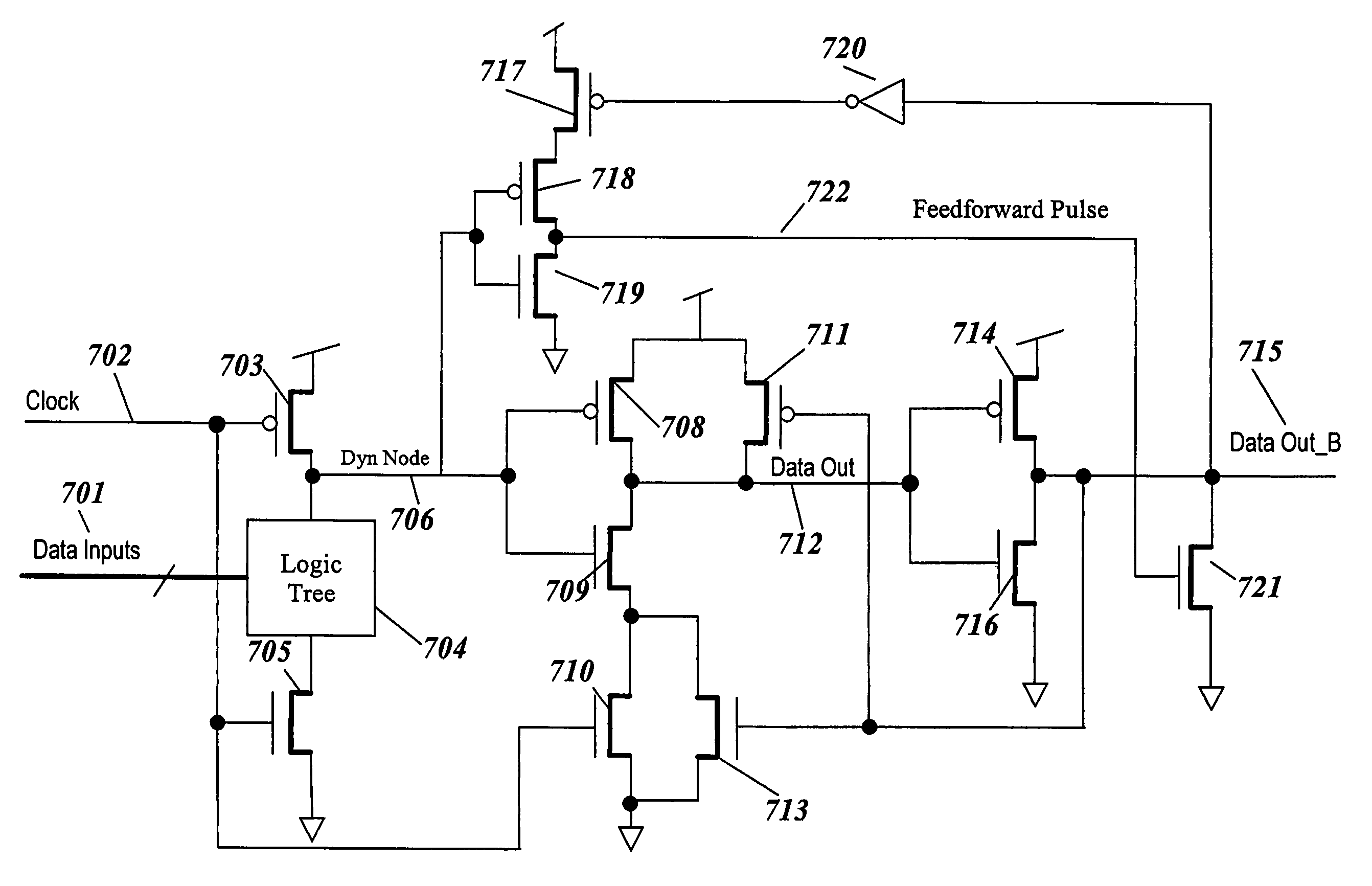
[0009]The pull down device in inverting data output stage of an LSDL gate is split into a large NFET and a small NFET. The large NFET is gated by a feedforward pulse that is generated only when the logic state of the inverting data output is a logic zero and the dynamic node evaluates to a logic zero. The dynamic node is coupled to a gated inverter that inverts the state of the dynamic node. If the inverting data output is a logic one, then an inverter inverts this state and enables the gated inverter. The output of the gated inverter generates a logic one feedforward pulse when the inverting data output is a logic one and the dynamic node evaluates to a logic zero. The logic one feedforward pulse turns ON the large NFET which quickly pulls the inverting data output to a logic zero. The small NFET acts as a keeper and is turned ON through the normal LSDL logic path. When the inverting data output is a logic zero, then the large NFET remains OFF reducing switching power and leakage power. Since the largest NFET in the feedforward LSDL logic gate is pulse driven, the remaining FET devices may be scaled down in size further reducing power as they in turn drive smaller devices. Even though additional circuitry is added for the gated inverter and the inverting stage there is a net reduction in device area and thus power savings.

Problems solved by technology

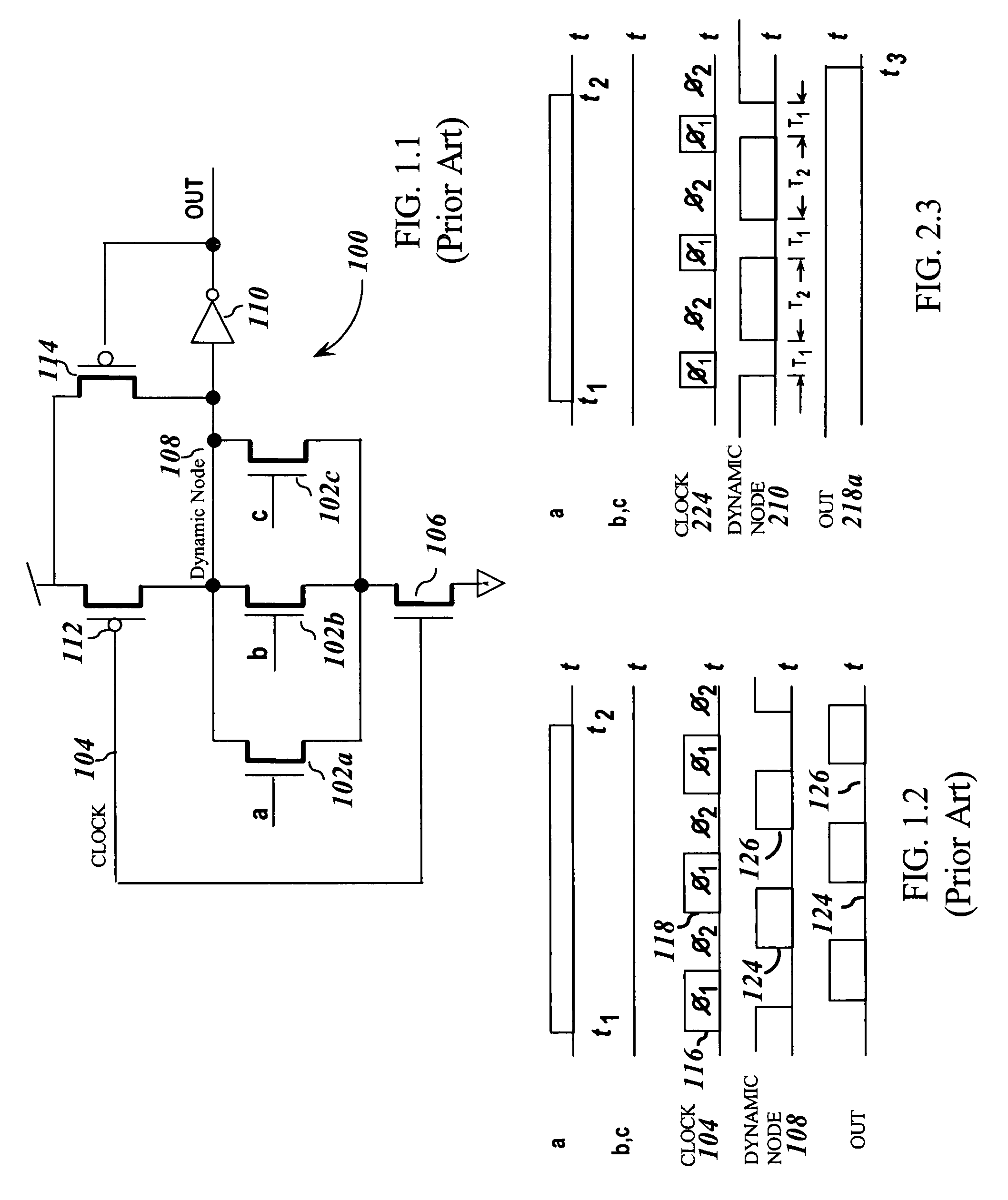
However, the switching of the output node with the toggling of the phase of the clock on each cycle may consume power even when the logical value of the output is otherwise unchanged.

Method used


Image

  • Feedforward limited switch dynamic logic circuit
  • Feedforward limited switch dynamic logic circuit
  • Feedforward limited switch dynamic logic circuit

Examples


Embodiment Construction

[0025]In the following description, numerous specific details are set forth to provide a thorough understanding of the present invention. However, it will be obvious to those skilled in the art that the present invention may be practiced without such specific details. In other instances, well-known circuits may be shown in block diagram form in order not to obscure the present invention in unnecessary detail. For the most part, details concerning timing, data formats within communication protocols, and the like have been omitted inasmuch as such details are not necessary to obtain a complete understanding of the present invention and are within the skills of persons of ordinary skill in the relevant art.

[0026]Refer now to the drawings wherein depicted elements are not necessarily shown to scale and wherein like or similar elements are designated by the same reference numeral through the several views.

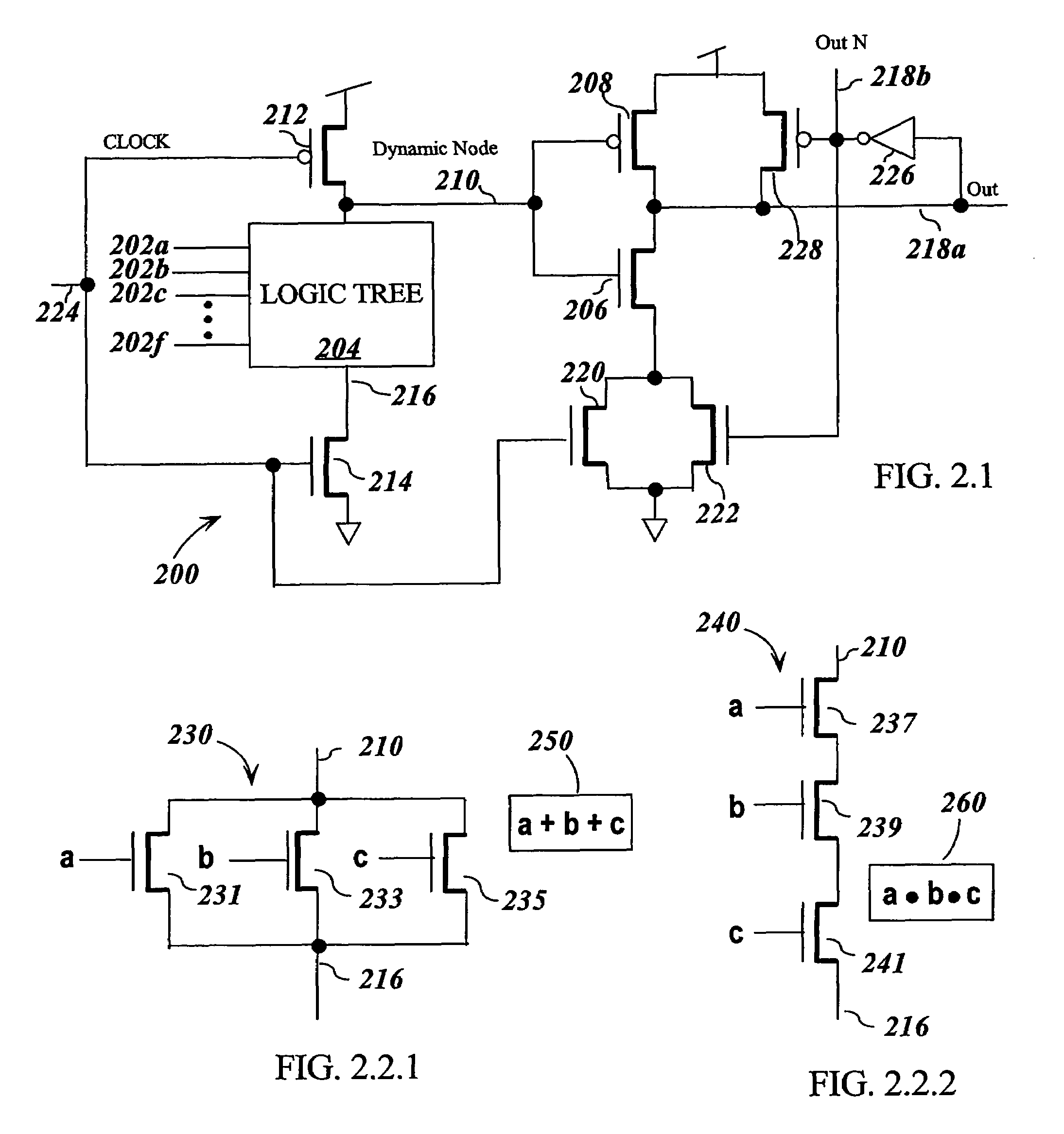
[0027]FIG. 2.1 illustrates a standard limited switch dynamic logic (LSDL) device 20...


PUM


Abstract

The N channel field effect transistor (NFET) of the inverting output stage of a LSDL gate is split into a large NFET and a small NFET. The large NFET is coupled to a feedforward pulse so that it is turned ON only when the inverting output is a logic one. When the inverting output is a logic one, another inverting stage turns ON if the dynamic node evaluates to a logic zero. The dynamic node is inverted and coupled to the large NFET on the inverting output stage thus quickly pulling the inverting output to a logic zero. The small NFET is turned ON as a keeper device through the normal logic path. If the inverting data output is a logic zero the feedforward pulse is not generated. By making the largest NFET a pulsed device the other FETs are reduced in size resulting in leakage and switching power savings.

Description

CROSS REFERENCE TO RELATED APPLICATION[0001]The present invention is related to U.S. patent application Ser. No. 10 / 116,612, filed Apr. 4, 2002, entitled “CIRCUITS AND SYSTEMS FOR LIMITED SWITCH DYNAMIC LOGIC,” which is incorporated by reference herein.TECHNICAL FIELD[0002]The present invention relates in general to metal oxide silicon (MOS) dynamic logic circuits.BACKGROUND INFORMATION[0003]Modem data processing systems may perform Boolean operations on a set of signals using dynamic logic circuits. Dynamic logic circuits are clocked. During the precharge phase of the clock, the circuit is preconditioned, typically by precharging an internal node (dynamic node) of the circuit by coupling to a power supply rail. During an evaluate phase of the clock, the Boolean function being implemented by the logic circuit is evaluated in response to the set of input signal values appearing on the inputs during the evaluate phase. (For the purposes herein, it suffices to assume that the input sig...

Claims


Application Information

Patent Timeline
Patent Type & Authority Patents(United States)
IPC IPC(8): H03K3/012H03K19/096H03K3/356H03K3/00
CPCH03K3/012H03K3/356121H03K19/0963
Inventor NGO, HUNG C.
Owner INT BUSINESS MASCH CORP
Learn More