Semiconductor device and method for the fabrication thereof

Inactive Publication Date: 2005-08-02
PANASONIC CORP
View PDF15 Cites 4 Cited by
  • Summary
  • Abstract
  • Description
  • Claims
  • Application Information

AI Technical Summary

Benefits of technology

[0026]In the semiconductor device of the present invention, external electrodes are formed on the insulation layer with which the major surface of the first semiconductor element and the backside surface of the second semiconductor element are coated, whereby a two-dimensional arrangement of external electrodes becomes possible to make. This therefore provides a semiconductor device on which a much greater number of external electrodes can be formed, when compared with the conventional semiconductor device using, as an external electrode, an external lead extracted from a lateral surface of the conventional semiconductor device. Further, the semiconductor device of the present invention differs from the conventional semiconductor device in using no lead frame, and in the semiconductor device of the present invention the external electrodes are formed on the insulation layer located on the major surface of the first semiconductor element, whereby the semiconductor device of the present invention can be of the size of the first semiconductor element. The present invention therefore provides a further down-sized semiconductor device than the conventional semiconductor device which is dimensionally constrained by the size of lead frame or the like. If external electrodes are formed on the insulation layer located on the backside surface of the second semiconductor element, this makes it possible to use the entire top surface of the semiconductor device for the layout of external electrodes.
[0032]In the case that both the insulation layer and the backside surface of the second semiconductor chip are ground and another insulation layer is formed on the ground insulation layer and on the ground backside surface of the second semiconductor chip, the planarity of the insulation layer is secured and the planarity of the external electrode is made good. Preparation of a semiconductor wafer in which a plurality of the first semiconductor elements have been formed makes it possible to carry out each of the fabrication steps in the semiconductor wafer state, therefore considerably reducing manufacturing costs.

Problems solved by technology

However, the conventional COC 100 has difficulties in being multipin-ized to a further extent.
Therefore, it is difficult to reduce the size of the COC 100.

Method used


Image

  • Semiconductor device and method for the fabrication thereof
  • Semiconductor device and method for the fabrication thereof
  • Semiconductor device and method for the fabrication thereof

Examples


embodiment 1

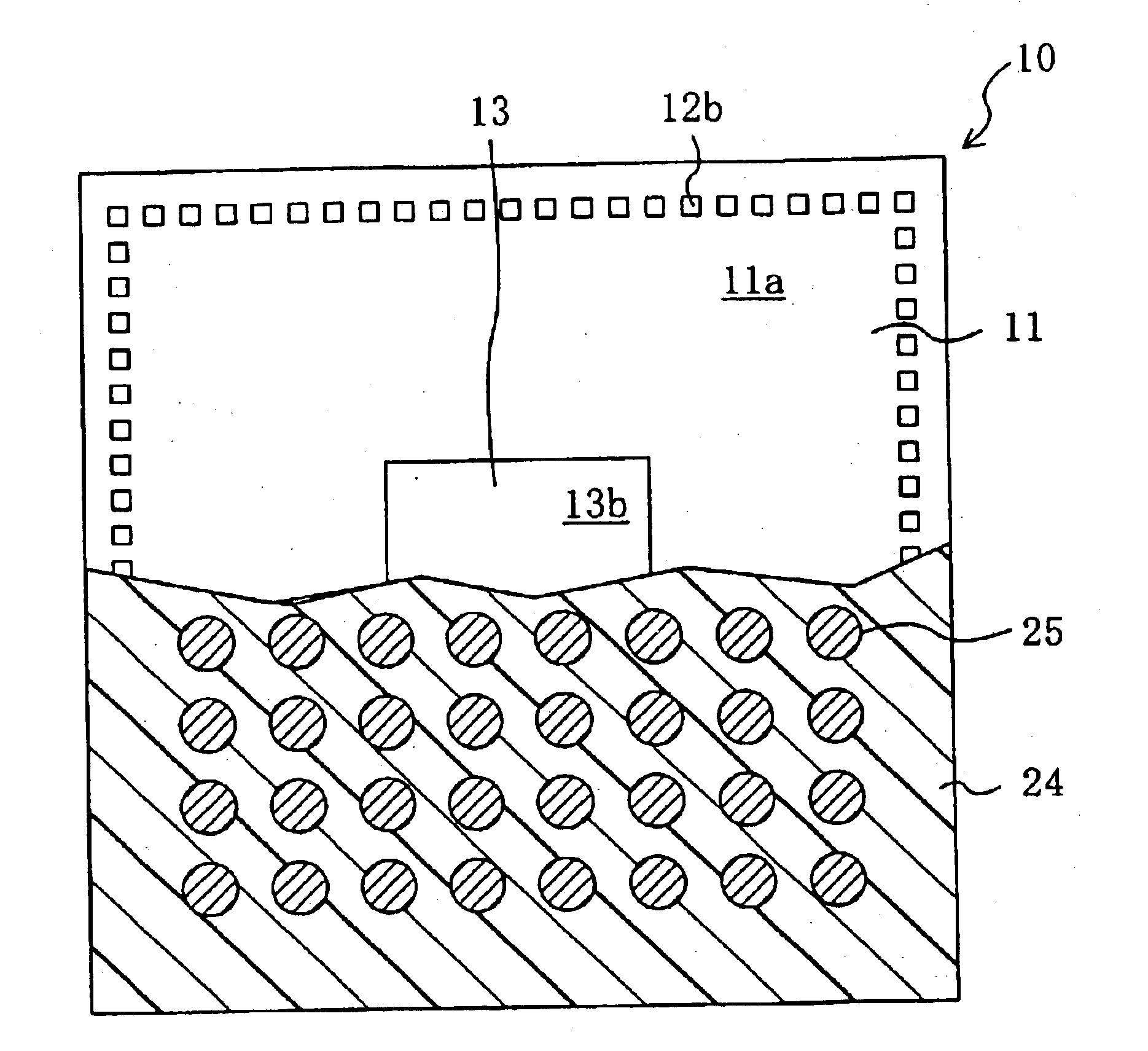
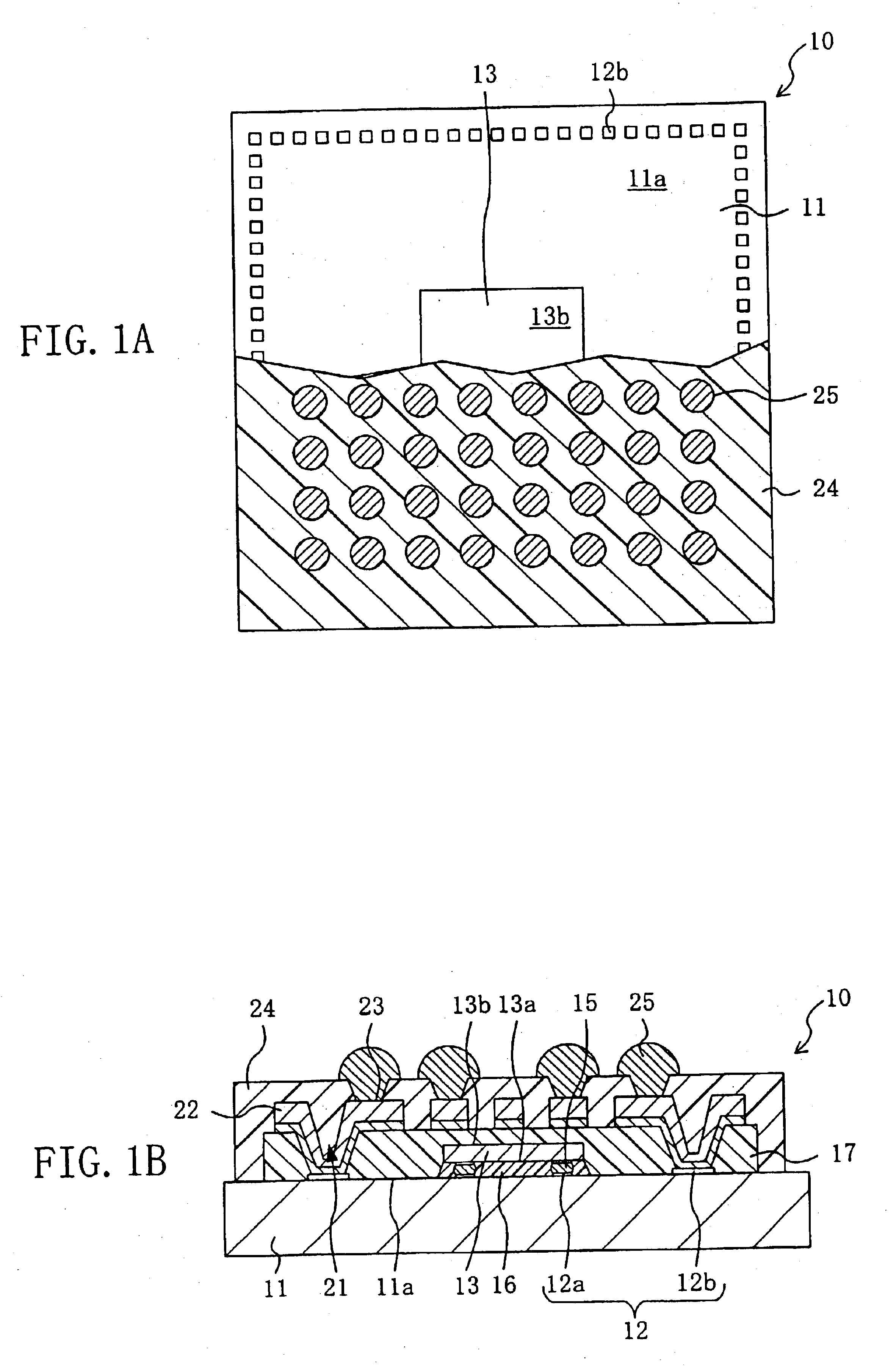
[0039]A first embodiment of the present invention will be described with reference to FIG. 1. FIG. 1A is a schematic of the top surface of the semiconductor device 10 according to the present embodiment. A portion of the semiconductor device 10 is cut away to provide an explanation of the internal structure of the semiconductor device 10. FIG. 1B schematically shows a cross section of the semiconductor device 10.

[0040]The semiconductor device 10 of the present embodiment includes a first semiconductor element (a first semiconductor chip) 11 having a major surface 11a on which a plurality of first element electrodes 12 are disposed, a second semiconductor element (a second semiconductor chip) 13 having a major surface 13a on which a plurality of second element electrodes 14 are disposed, an insulation layer 17 formed on the major surface 11a of the first semiconductor chip 11 so as to cover the second semiconductor chip 13, and a wiring layer 22 formed on the insulation layer 17. The...

embodiment 2

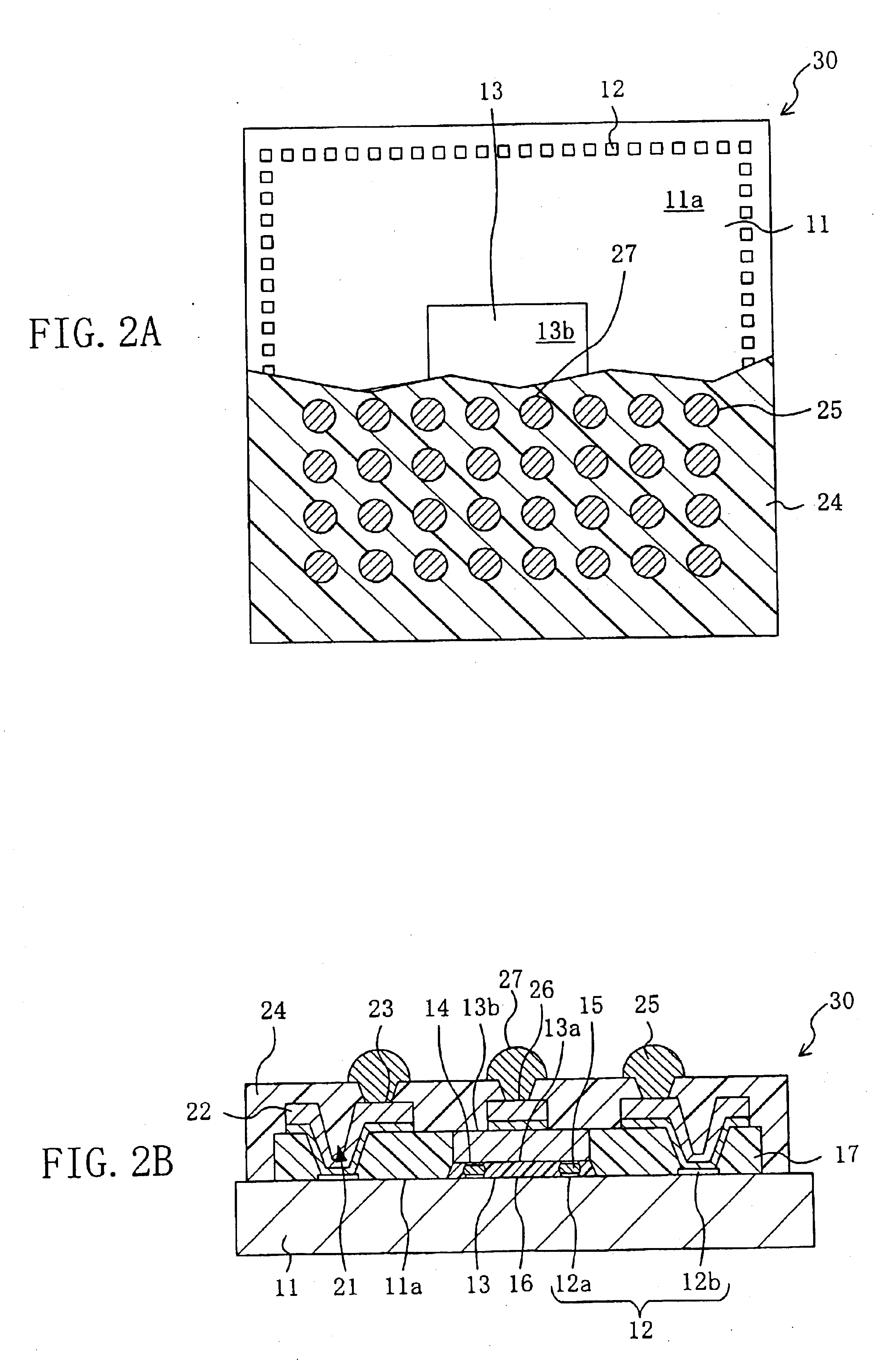
[0056]Hereinafter, a method for the fabrication of a semiconductor device according to a second embodiment of the present invention will be described with reference to FIGS. 3A-3G and FIGS. 4A-4G. FIGS. 3A-3G and FIGS. 4A-4G illustrate in cross section respective steps of the semiconductor device fabrication method of the present embodiment.

[0057]First, as shown in FIG. 3A, a semiconductor wafer 50 is prepared. The semiconductor wafer 50 includes a plurality of the first semiconductor chips 11 on which the first element electrodes 12 are formed. Not the semiconductor wafer 50 but the first semiconductor chip 11 in the chip state may be prepared.

[0058]Next, as shown in FIG. 3B, the connection member 15, made of, for example, solder or conductive paste, is formed on the second element electrode 14 of the second semiconductor chip 13. Thereafter, the second element electrode 14 of the second semiconductor chip 13 is placed, through the connection member 15, onto the first element elect...


PUM


Abstract

Disclosed is a semiconductor device 10 comprising a first semiconductor element 11 with an arrangement of first element electrodes 12, a second semiconductor element 13 with an arrangement of second element electrodes 14, a connection member 15 electrically connecting together a portion 12b of the first element electrodes 12 and the second element electrodes 14, an insulation layer 17 covering a major surface 11a of the first semiconductor element 11 and a backside surface 13b of the second semiconductor element 13, a wiring layer 22 formed on the insulation layer 17 and electrically connected to the first element electrode portion 12b exposed in an opening portion 21, and an external electrode 23 formed, as a portion of the wiring layer 22, on the insulation layer 17.

Description

[0001]This application is a divisional of prior U.S. application Ser. No. 09 / 785,503 filed Feb. 20, 2001, now U.S. Pat. No. 6,559,528.BACKGROUND OF THE INVENTION[0002]The present invention relates to a semiconductor device provided with semiconductor elements and to a method for the fabrication of such a semiconductor device. The present invention relates more particularly to a semiconductor device protecting its semiconductor elements and securing establishment of electrical connections between the semiconductor elements and external equipment.[0003]In recent years, since electronic equipment is becoming smaller and smaller in size and being highly improved in function, there have been strong demands for improvement in packaging density as well as the miniaturization and the high operation rate of the semiconductor device. In order to meet these demands, various forms of packaging have been developed. For example, the COC (Chip On Chip) module has been developed as a packaging form...

Claims


Application Information

Patent Timeline
IPC IPC(8): H01L25/065H01L23/28H01L23/31H01L23/498H01L23/48H01L25/18H01L25/07
CPCH01L23/3114H01L23/3121H01L23/49872H01L24/97H01L25/0657H01L24/94H01L2224/16145H01L2224/48091H01L2224/48247H01L2224/48465H01L2224/97H01L2225/06513H01L2225/06524H01L2225/06527H01L2225/06582H01L2225/06586H01L2924/01004H01L2924/01029H01L2924/01074H01L2924/01078H01L2924/01079H01L2924/01082H01L2924/14H01L2924/00014H01L2224/81H01L2924/01005H01L2924/01006H01L2924/01024H01L2924/01033H01L2924/00H01L24/48H01L2224/73204H01L2224/32145H01L2924/00012H01L2224/94H01L2224/12105H01L2924/351H01L2924/12042H01L24/45H01L2224/05599H01L2224/45144H01L2224/85399H01L2224/73209H01L2224/05573H01L2224/05568H01L2224/05647H01L2924/181H01L2224/06131H01L2224/023H01L2924/00015H01L2224/45015H01L2924/207H01L2924/0001H01L23/48
Inventor WATASE, KAZUMIFUJIMOTO, HIROAKISAHARA, RYUICHISHIMOISHIZAKA, NOZOMIKUMAKAWA, TAKAHIROKAINO, KAZUYUKINAKAMURA, YOSHIFUMI
Owner PANASONIC CORP
Why Eureka
Try Eureka