

Method and apparatus for testing BGA-type semiconductor devices
a technology of semiconductor devices and methods, applied in the direction of electronic circuit testing, measurement devices, instruments, etc., can solve the problems of pocket size, difficulty in picking up the semiconductor device from the pocket, contact failure or deformation failure of the bump terminal,
- Summary
- Abstract
- Description
- Claims
- Application Information
AI Technical Summary
Benefits of technology
Problems solved by technology
Method used
Image

Examples
Embodiment Construction
[0034]This invention was first disclosed in Japanese Patent Application No. 2002-306751, which is incorporated herein by reference in its entirety.
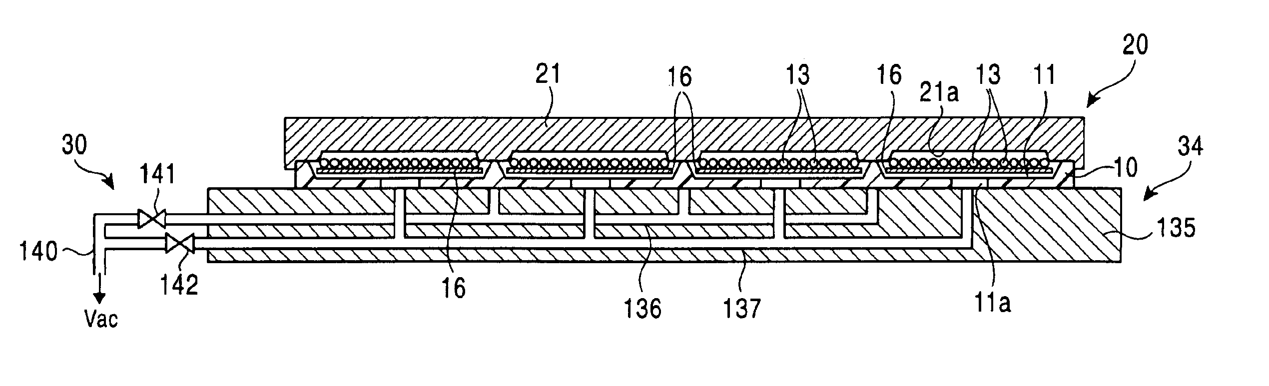
[0035]In various exemplary embodiments of this invention, a testing apparatus has a terminal-position adjusting unit, a fixing unit, a moving unit, and a test head.
[0036]This exemplary testing apparatus receives a plurality of semiconductor devices placed in respective pockets of a tray with their respective terminal surfaces facing upward. In various exemplary embodiments of this invention, the terminal-position adjusting unit adjusts positions of bump terminals on the semiconductor devices. In various exemplary embodiments of this invention, when the adjustment is completed, the fixing unit detachably fixes the semiconductor devices to the tray. Then, in various exemplary embodiments of this invention, the moving unit moves the tray such that the bump terminals of the semiconductor devices in the tray are successively positioned at a pr...
PUM
 Abstract
Description
Claims
Application Information