Integrated logic circuit and hierarchical design method thereof

a logic circuit and logic gate technology, applied in logic circuits using specific components, pulse techniques, instruments, etc., can solve the problems of weak logic gates in driving capability, complicated configuration, and large so as to reduce the number of timing-adjusting positions, simplify the configuration of connections, and shorten the design period

Inactive Publication Date: 2005-08-02
SOCIONEXT INC
View PDF2 Cites 0 Cited by
  • Summary
  • Abstract
  • Description
  • Claims
  • Application Information

AI Technical Summary

Benefits of technology

[0005]Therefore, it is an object of the present invention to provide an integrated logic circuit and a hierarchical design method thereof which simplifies the configuration of connections between modules of the top level and reduces the number of timing-adjusting positions, so as to shorten the design period.
[0007]According to this configuration, input and output of signals between the internal and external circuits of the module is made always through the external buffer cells of the module, thereby simplifying the configuration of connection, reducing the number of timing-error adjusting positions, and reducing the number of repeated times of timing-error checking and layout correcting processes, compared with the prior art, in result of shortening the design period.

Problems solved by technology

On the other hand, as the circuit components become smaller in size, logic gates become weaker in driving capability, and several repeater cells (buffer gates) must be inserted on the route for wiring a long path between modules.
For this reason, the configuration becomes complicated, the number of timing-adjusting positions becomes larger, and timing-error checking and layout correcting are required so many repeated times, in result of extending the design period of semiconductor logic circuit.

Method used


Image

  • Integrated logic circuit and hierarchical design method thereof
  • Integrated logic circuit and hierarchical design method thereof
  • Integrated logic circuit and hierarchical design method thereof

Examples


Embodiment Construction

[0019]Hereinafter, the present invention will be described in more detail referring to the drawings.

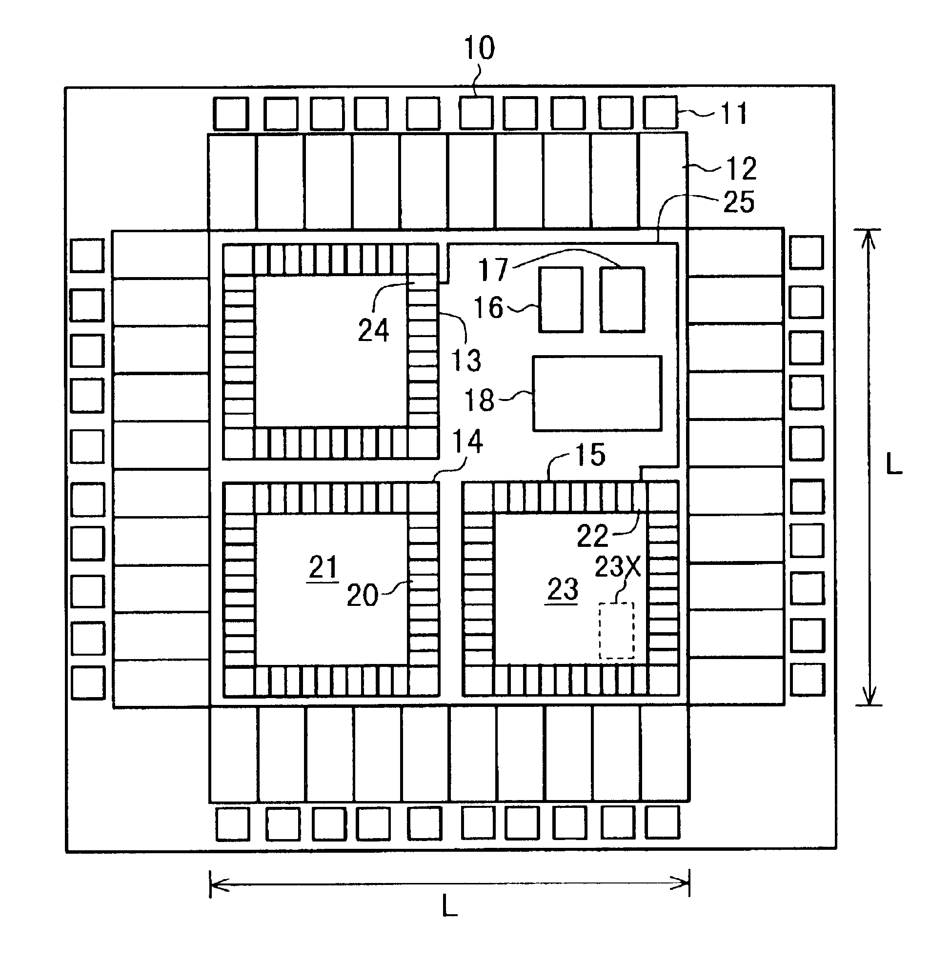
[0020]FIG. 1 is a view showing an arrangement of modules of the top level in hierarchical design of a chip 10 where an integrated logic circuit is formed.

[0021]A plurality of pads 11 are disposed along the periphery of the chip 10, I / O cells 12 are formed corresponding to each of the plurality of pads 11, and modules 13 to 18 are formed inside the plurality of I / O cells 12.

[0022]The modules 16 to 18 belong to the conventional hard macro and have been optimized in design, and the positions of not-shown terminals of the top level have been fixed.

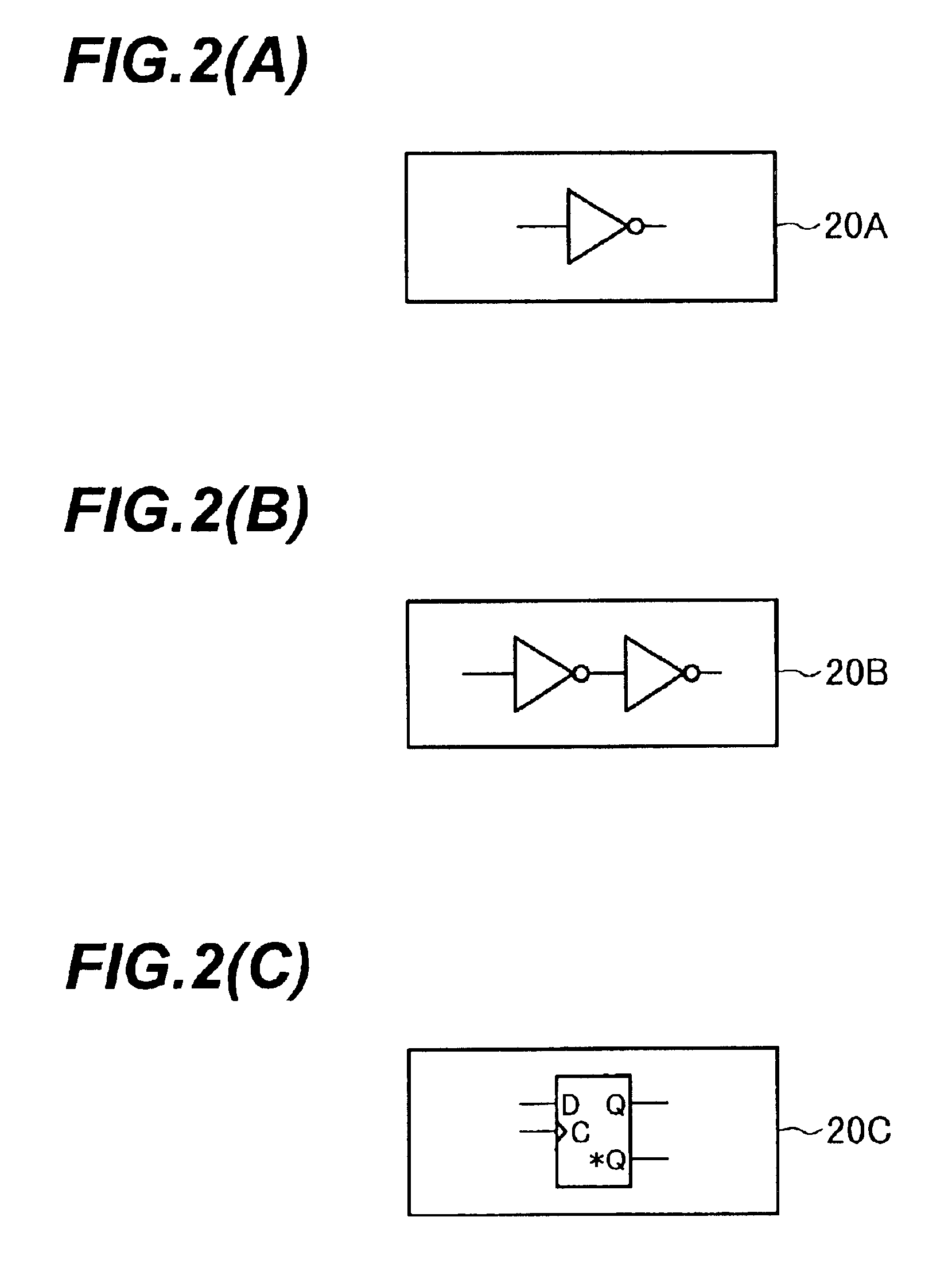
[0023]On the other hand, each of modules 13 to 15 has a featured configuration according to this embodiment of the present invention. For example, the module 14 includes a plurality of external buffer cells 20 disposed along the periphery thereof and an internal circuit 21 disposed inside the buffer cells 20, and through the buffer cells 20, inp...


PUM


Abstract

Modules 14 to 18 are disposed in a chip 10, and the module 14 includes a plurality of external buffer cells 20 disposed along the peripheral of the module 14, and an internal circuit 21 disposed inside the plurality of external buffer cells 20. Input and output of signals is made between the internal circuit 21 and the external circuit, through the external buffer cells 20. The output-stage transistor of each external buffer cell has a larger size than the transistor size of the internal circuit 21. The external buffer cells 20 have a driving capability for enabling direct driving of a transistor inside the chip through a wire having the maximum Manhattan length of a module-disposed region in on chip. If the disposed area of the plurality of external buffer cells 20 is not sufficient, the size of the module is enlarged, or repartition is made to reform the modules so that the plurality of external buffer cells 20 have their sufficient disposed area.

Description

BACKGROUND OF THE INVENTION[0001]1. Field of the Invention[0002]The present invention relates to an integrated logic circuit provided with modules and a hierarchical design method thereof.[0003]2. Description of the Related Art[0004]As an integrated logic circuit has been developed to have higher efficiency and larger scale, there occurs a case where thousands of input and Output-stages are included in the top level of hierarchical design. On the other hand, as the circuit components become smaller in size, logic gates become weaker in driving capability, and several repeater cells (buffer gates) must be inserted on the route for wiring a long path between modules. For this reason, the configuration becomes complicated, the number of timing-adjusting positions becomes larger, and timing-error checking and layout correcting are required so many repeated times, in result of extending the design period of semiconductor logic circuit.SUMMARY OF THE INVENTION[0005]Therefore, it is an obj...

Claims


Application Information

Patent Timeline
Patent Type & Authority Patents(United States)
IPC IPC(8): G06F17/50H03K19/177H01L21/82H01L21/822H01L27/04
CPCG06F17/5068H03K19/17736H03K19/17744H03K19/1778G06F30/39H01L2224/05554
Inventor SUZUKI, KENJIOSAJIMA, TORUTAJIMA, SHOGOSATOH, SHIGENOBU
Owner SOCIONEXT INC
Why Eureka
Try Eureka