

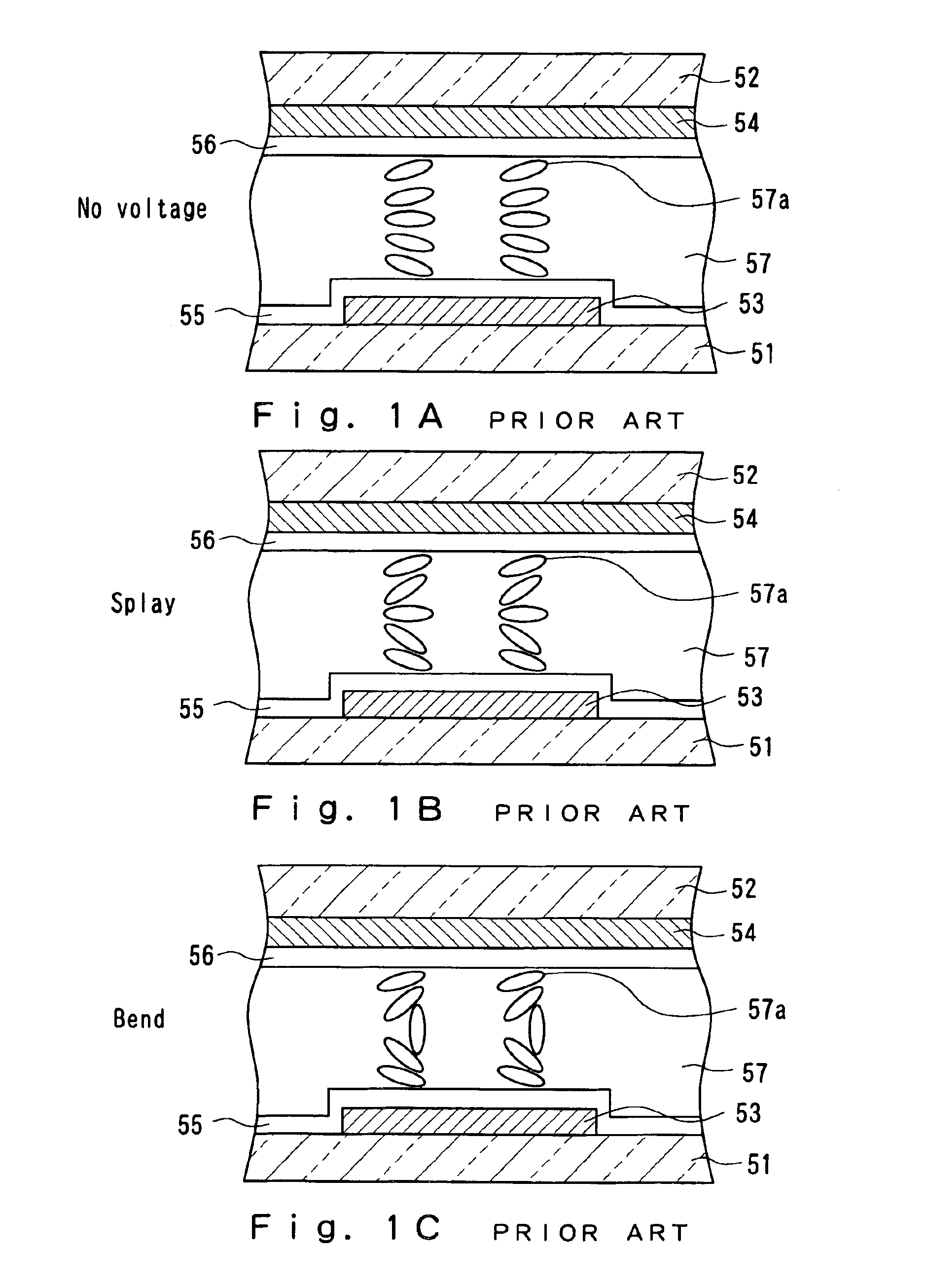
Liquid crystal display using liquid crystal with bend alignment and driving method thereof
a technology of bend alignment and liquid crystal, applied in the direction of liquid crystal compositions, instruments, chemistry apparatus and processes, etc., can solve the problems of slow response time, significant difference in response time, and inability to fully understand the physical mechanism of bend transition, etc., and achieve the effect of fast response tim
- Summary
- Abstract
- Description
- Claims
- Application Information
AI Technical Summary
Benefits of technology
Problems solved by technology
Method used
Image

Examples
embodiment 1
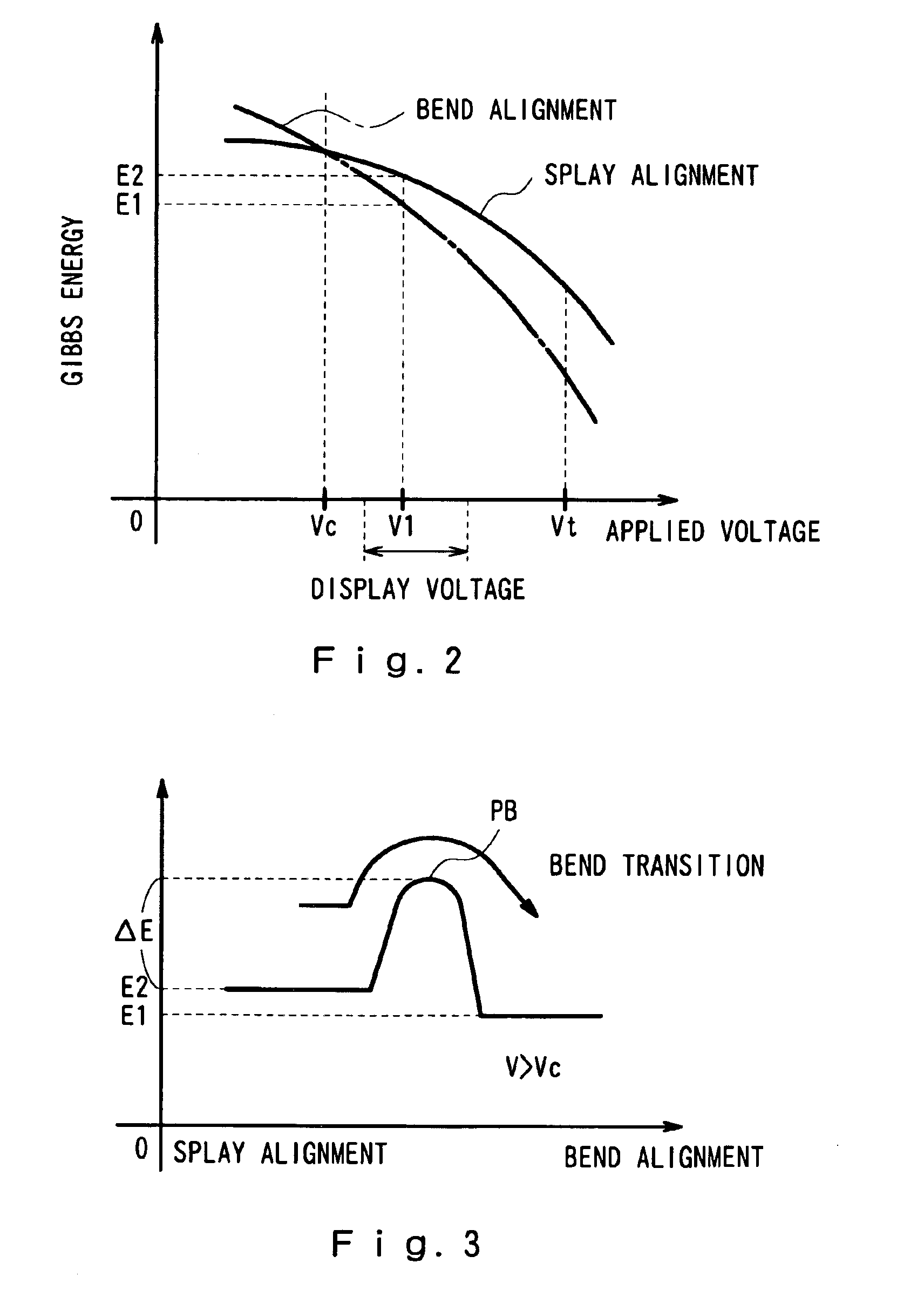
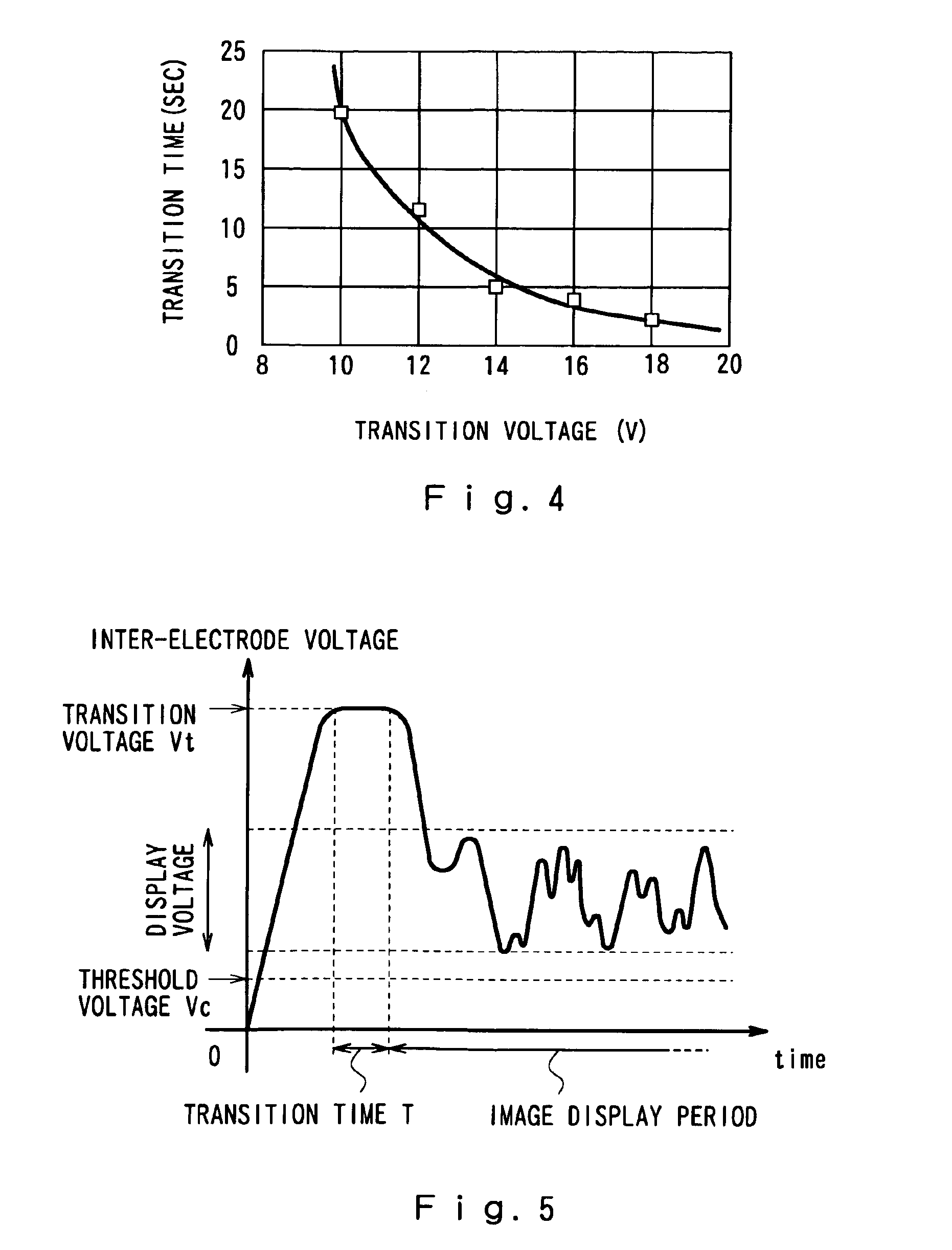
[0065]Specifically, if a transition voltage is once applied when an LCD is powered on, for example, to cause a bend transition in liquid crystal, the bend alignment state is maintained while a display voltage is applied (namely, while image display is performed). Therefore, in an LCD according to this embodiment using an OCB mode, a transition voltage Vt is first applied between the first and second electrodes for a transition time T when the LCD is powered on (time=0), and thereafter a display voltage in accordance with the waveform of a video signal is applied to perform image display, as in prior art LCDs. The transition voltage Vt and the transition time T may be determined based on FIG. 4, for example.
[0066]In order to secure a bend transition of liquid crystal, the values of a transition voltage Vt and a transition time T are determined by selecting, among the values for Vt and T plotted on a chart of FIG. 4, those existing in a region above the solid line. However, a long tra...
embodiment 2
[0075]A relationship between a bend transition and a distance between electrodes (an inter-electrode distance) in a passive matrix type LCD will now be described. FIGS. 7A to 7C are plan views depicting a transition from a splay alignment to a bend alignment in a passive matrix type LCD. The LCD comprises first and second transparent substrates facing each other which are made of glass, and liquid crystal interposed between the cell of these electrodes. A plurality of first electrodes 1 are formed on a surface of the first transparent substrate facing the second substrate so as to extend in the horizontal direction in a stripe shape. A plurality of second electrodes 2 are formed on a surface of the second transparent substrate facing the first substrate so as to extend in the vertical direction in a stripe shape. Regions where the first and second electrodes overlap with each other via liquid crystal form respective pixel regions 3, in which an electrical field is generated by a vol...
embodiment 3
[0097]A relationship between a bend transition and a pretilt angle will now be described with reference to an active matrix type LCD as an example. FIGS. 12A to 12C are plan views of an active matrix type LCD showing a transition from a splay alignment to a bend alignment. The structure of the LCD shown in FIGS. 12A to 12C is similar to the above described structure shown in FIGS. 6A and 10A.
[0098]Referring to FIG. 12A, each of several points 6 in cells indicated by cross hatched lines is a transition factor (transition source) which triggers a bend transition. As in the passive matrix type LCD shown in FIGS. 9A to 9C, in an active matrix type LCD, a bend transition occurs with these transition sources 6 as starting points and expands in the radial directions, which is shown in FIG. 12B. Referring to FIG. 12B, a bend transition is performed in hatched regions 5 which enlarges with time with the transfer source 6 as a center point, to finally expand over the entire surface of the cel...
PUM
| Property | Measurement | Unit |
|---|---|---|
| transition voltage | aaaaa | aaaaa |
| width | aaaaa | aaaaa |
| width | aaaaa | aaaaa |
Abstract
Description
Claims
Application Information