Semiconductor memory device having an internal voltage generation circuit for selectively generating an internal voltage according to an external voltage level

Inactive Publication Date: 2005-08-16
SAMSUNG ELECTRONICS CO LTD
View PDF10 Cites 27 Cited by
  • Summary
  • Abstract
  • Description
  • Claims
  • Application Information

AI Technical Summary

Benefits of technology

[0014]Embodiments of the invention provide a semiconductor memory device that can simply manage a database irrespective of the level of an external voltage and reduce a mask making expenditure. Embodiments of the invention also provide a semiconductor memory device that can stably generate an internal voltage according to the level of an external voltage.

Problems solved by technology

Independently managing the first and second database is troublesome and may cause an error in selection of database for revision.
In addition, mask sets must be managed independently according to the first and second database, which leads to the disadvantage of high cost.
Unfortunately, the internal voltage generation circuit 130 is incapable of stably maintaining the level of the internal voltage VINT.

Method used


Image

  • Semiconductor memory device having an internal voltage generation circuit for selectively generating an internal voltage according to an external voltage level
  • Semiconductor memory device having an internal voltage generation circuit for selectively generating an internal voltage according to an external voltage level
  • Semiconductor memory device having an internal voltage generation circuit for selectively generating an internal voltage according to an external voltage level

Examples


Embodiment Construction

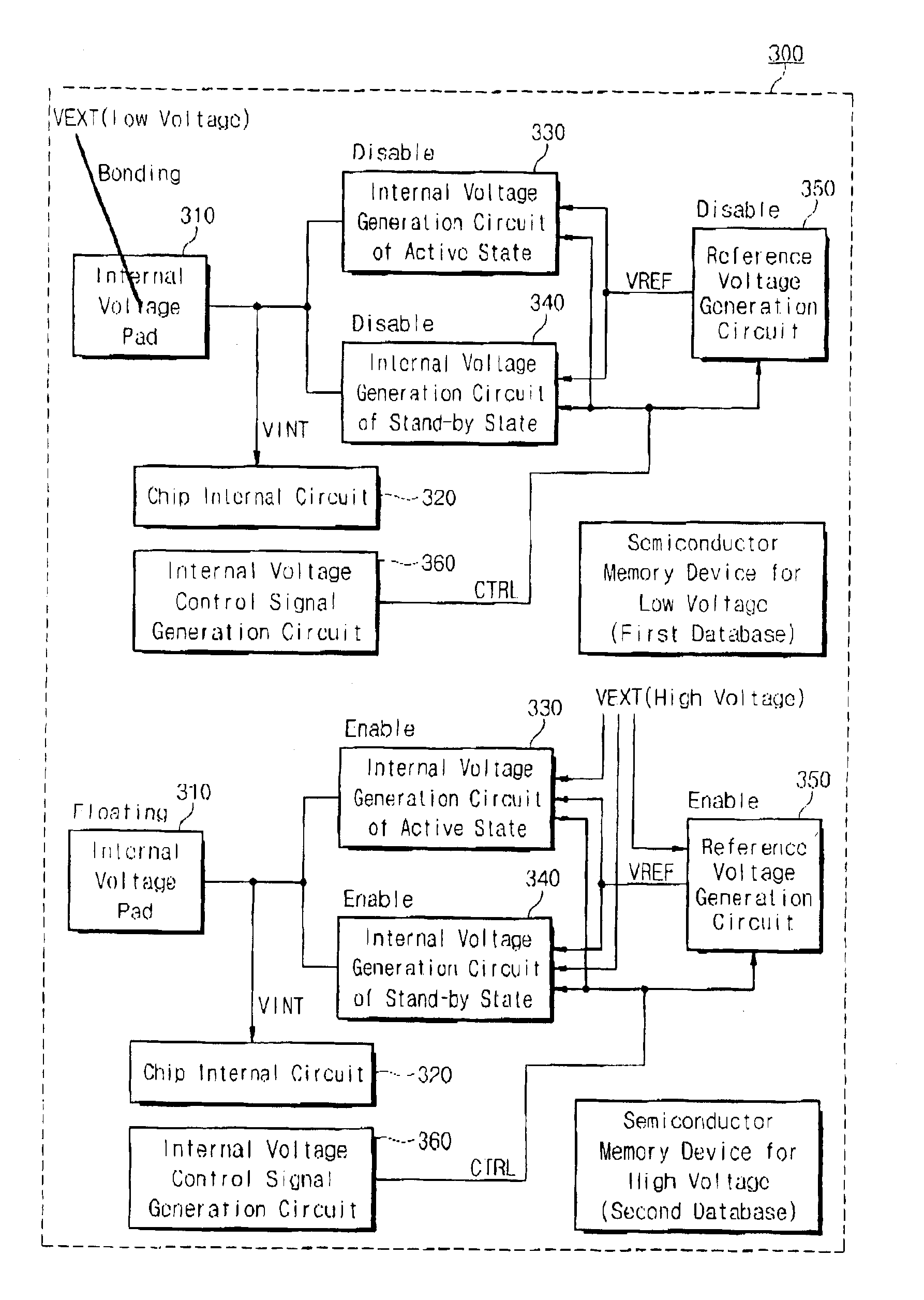
[0030]A semiconductor memory device according to an embodiment of the invention is now described below with reference to FIG. 3.

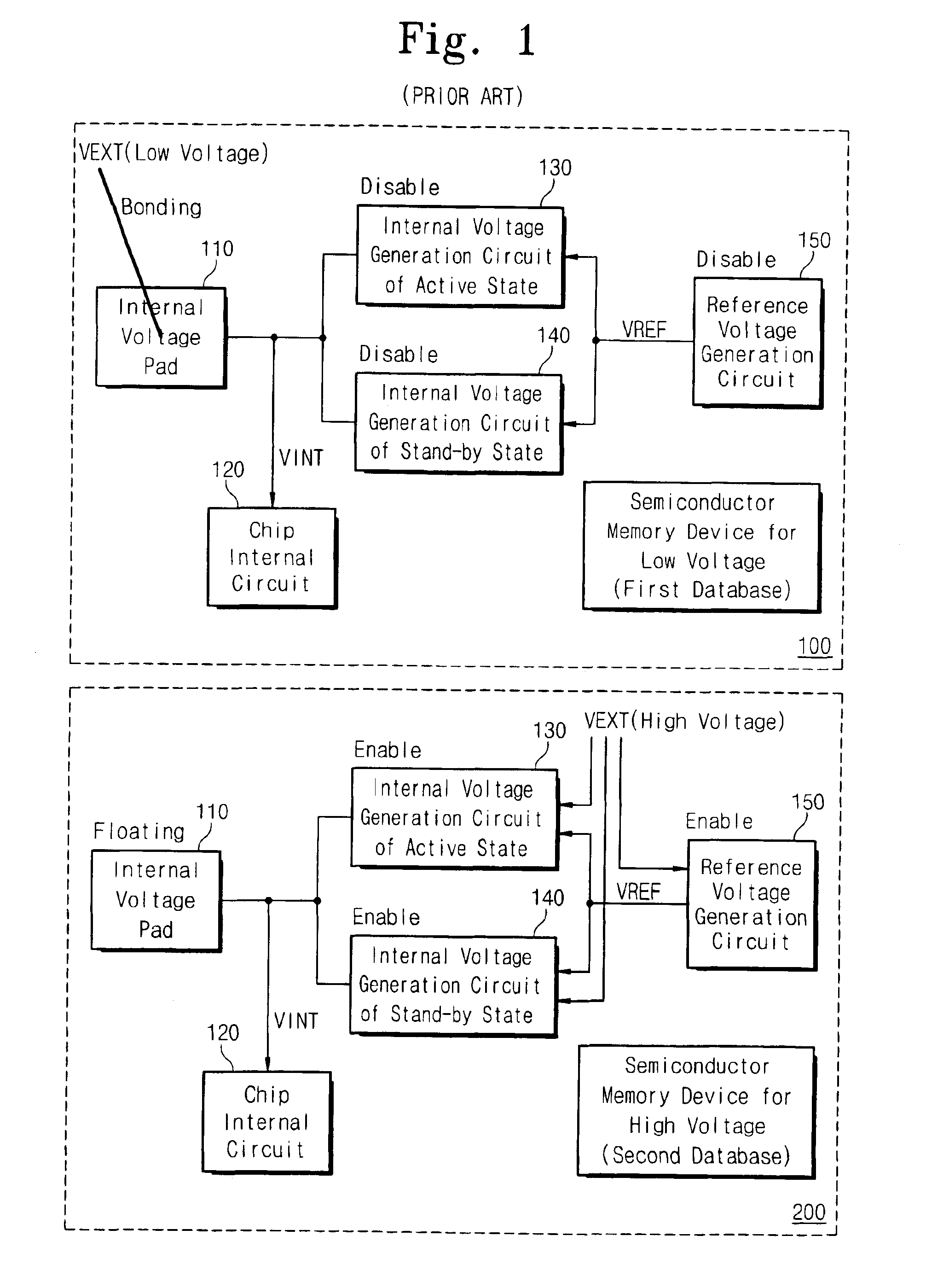
[0031]Referring to FIG. 3, a semiconductor memory device includes an internal voltage pad 310 having one database, a chip internal circuit 320, an internal voltage generation circuit 330 of an active state, an internal voltage generation circuit 340 of a stand-by state, a reference voltage generation circuit 350, and an internal voltage control signal generation circuit 360. The semiconductor memory device 300 is different from the semiconductor memory devices 100 and 200 in that it further includes the internal voltage control signal generation circuit 360.

[0032]The internal voltage control signal generation circuit 360 is now explained in detail with reference to FIG. 4 and FIG. 5.

[0033]Referring to FIG. 4, an internal voltage control signal generation circuit 360 according to an embodiment of the invention includes a first driver 402 having a PMOS transi...


PUM


Abstract

An external high / low voltage compatible semiconductor memory device includes an internal voltage pad, an internal voltage generation circuit, and an internal voltage control signal generation circuit. The internal voltage pad connects a low external voltage with an internal voltage, and the internal voltage generation circuit generates an internal voltage in response to an internal voltage control signal and a high external voltage. The internal voltage control signal generation circuit generates an internal voltage control signal according to an high or low external voltage. Thus, a database of the semiconductor memory device can be managed without classifying the database into databases for the high voltage and databases for the low voltage because of the internal voltage control signal. In addition, the internal voltage level is stable because charges provided to the internal voltage are regulated according to a voltage level of the external voltage.

Description

CROSS REFERENCE TO RELATED APPLICATIONS[0001]This application claims priority from Korean Patent Application No. 2002-41543, filed on Jul. 16, 2002, the contents of which are hereby incorporated by reference in their entirety for all purposes.BACKGROUND OF THE INVENTION[0002]1. Technical Field of the Invention[0003]This disclosure relates to a semiconductor memory device and, more specifically, to a semiconductor memory device having an internal voltage generation circuit for selectively generating an internal voltage according to an external voltage level.[0004]2. Description of the Related Art[0005]In semiconductor memory devices for use in mobile apparatuses, low voltage operation is the most significant factor. The design of a low voltage semiconductor memory device varies according to the external voltage used. For example, if an external voltage is a high voltage, an internal voltage generation circuit is employed to lower the high voltage and the lowered voltage is used as an...

Claims


Application Information

Patent Timeline
IPC IPC(8): G11C5/14
CPCG11C5/147G11C5/14
Inventor LEE, KYU-CHANRHEE, SANG-JAECHOI, JUNG-YONGCHOI, JONG-HYUNNA, JONG-SIKKIM, JAE-HOON
Owner SAMSUNG ELECTRONICS CO LTD
Why Eureka
Try Eureka