Algorithms tunning for dynamic lot dispatching in wafer and chip probing

a technology of wafer and chip probing and algorithm tuning, applied in the field of semiconductor foundry dispatching system, can solve problems such as misoperation, and achieve the effect of efficient selection of work lots

Inactive Publication Date: 2005-08-16
TAIWAN SEMICON MFG CO LTD
View PDF18 Cites 12 Cited by
  • Summary
  • Abstract
  • Description
  • Claims
  • Application Information

AI Technical Summary

Benefits of technology

[0008]The overall objective of this invention is to create a comprehensive method and system for the dynamic adjustment of priority and step procedures for determining effective lot dispatching for wafer and chip probing in a semiconductor testing and manufacturing facility. A more specific objective is to create a two-phased, event-driven dispatching system structure for dynamic adjustment. Using step procedures, another objective is to efficiently choose work lots that can utilize incorporated auxiliary apparatus without the need for a costly new setup.
[0009]Additionally, yet another objective is to provide for the use of an engineering lot capacity limitation check in the step procedure to see if the amount of fixed testing time per week determined by testing site personnel for engineering lots to be tested on any particular machine has been exceeded. Another objective is to be able to solve the dispatching conflict between wafer and package lots. A final objective is to limit a tester's capability in product through the use of a common constraint system so that a wrong lot list can not be dispatched for a tester resulting in a mistake operation.

Problems solved by technology

A final objective is to limit a tester's capability in product through the use of a common constraint system so that a wrong lot list can not be dispatched for a tester resulting in a mistake operation.

Method used


Image

  • Algorithms tunning for dynamic lot dispatching in wafer and chip probing
  • Algorithms tunning for dynamic lot dispatching in wafer and chip probing
  • Algorithms tunning for dynamic lot dispatching in wafer and chip probing

Examples


Embodiment Construction

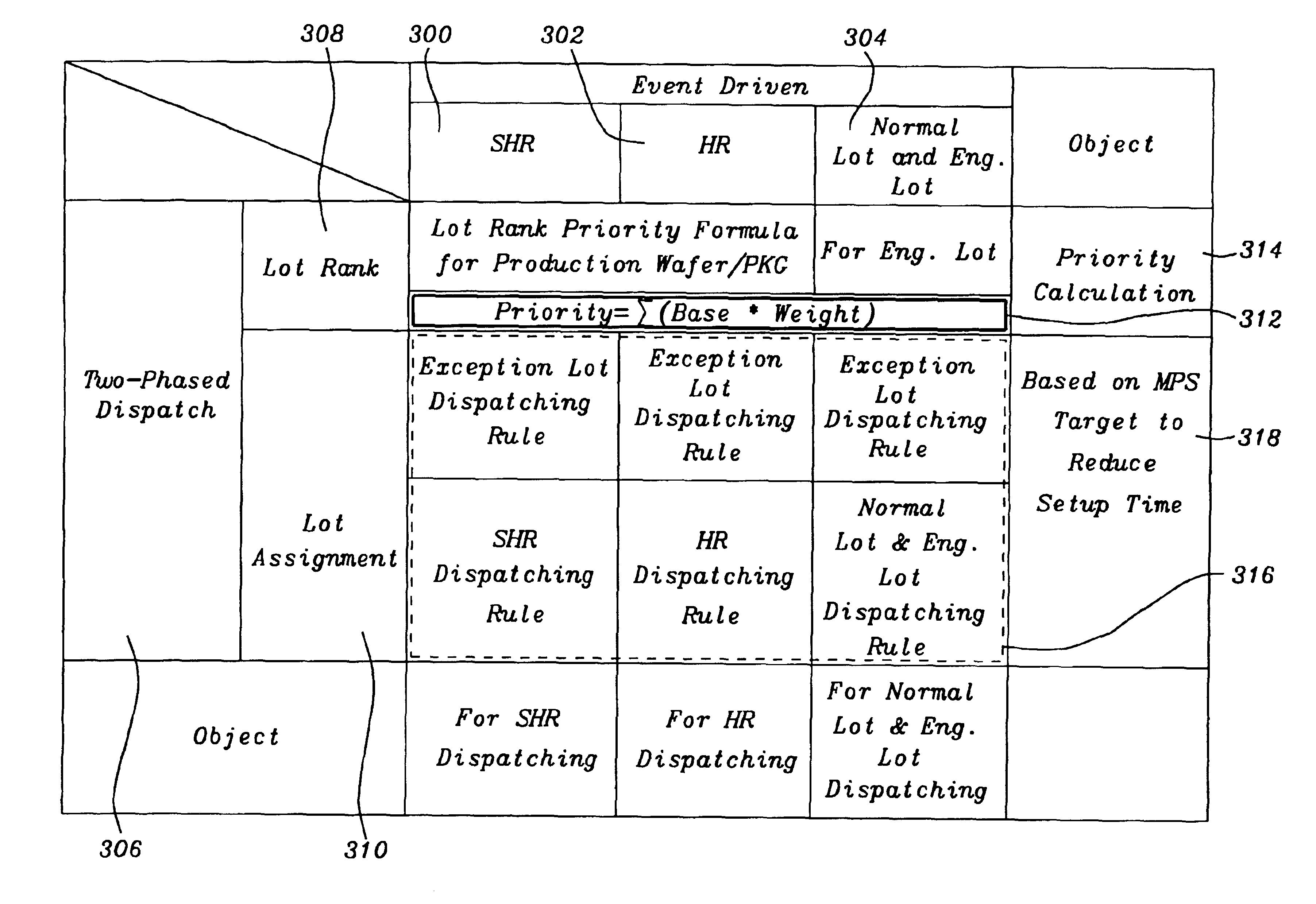
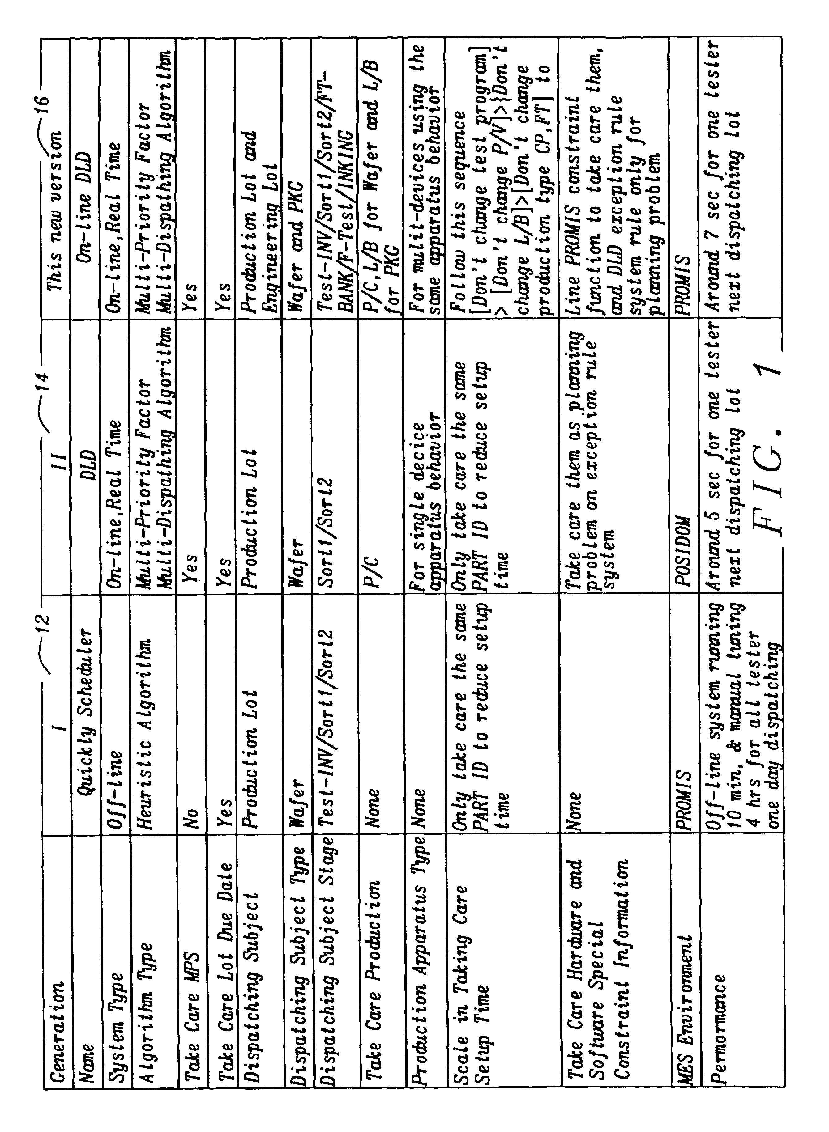
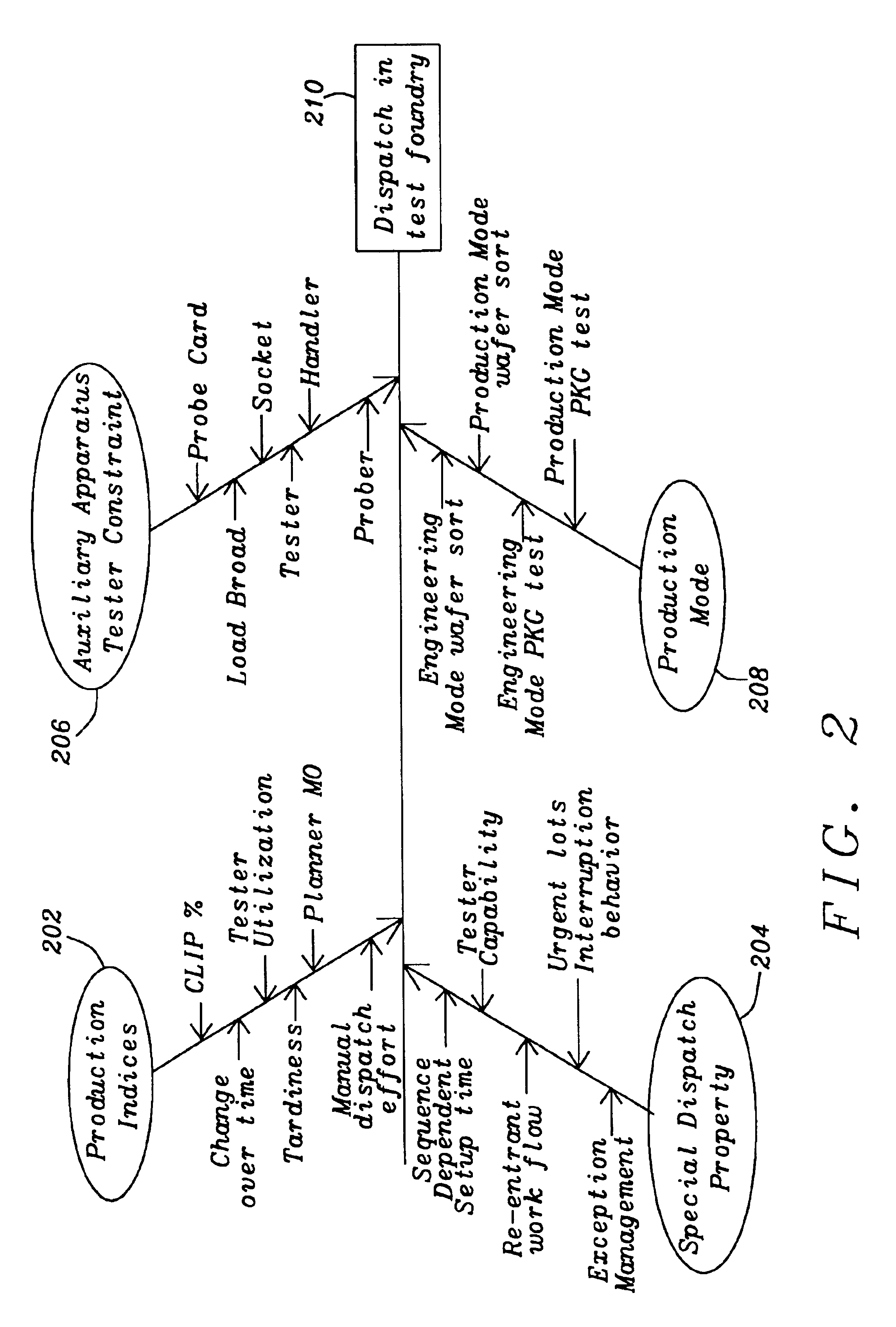
[0017]In the past, the main task of the test foundry planner was to prepare a lot dispatching sheet that showed lot assignment sequence on every tester for the next day on the shop floor as can be seen in the Quickly Scheduler column 12 of the comparison of three versions of scheduling / dispatching systems for testing chart of FIG. 1. In order to get a good dispatching result, the planner had to collect all the related Work in Progress (WIP) and production information such as basic engineering records of product, parameter value of the lots from the Manufacturing Execution System (MES), production target or Master Production Schedule (MPS) that Production Control (PC) provided, and the related auxiliary apparatus of the product from the material control system in advance every day. Taking into consideration the running situation of every tester, current production target execution status, and production strategies developed in daily meetings, the planner spent a great deal of time co...


PUM


Abstract

A method and system for flexible, comprehensive, on-line, real-time dynamic lot dispatching in a semiconductor test foundry based on a two-phased, event-driven dispatching system structure. An adjustable priority formula and tuned algorithms integrated with PROMIS' constraint function give a nearly optimum dispatching list on any tester at any time with reduced mistake operations. Exception rules take care of special events to improve daily dispatching manual effort. This invention can automatically dispatch engineering lots according to engineering lots' capacity of Testing, solve conflict between wafer and package lots, efficiently reduce tester setup times, replace daily manual-dispatching sheet and keep a high CLIP rate while fully following MPS.

Description

BACKGROUND OF THE INVENTION[0001]1. Field of Invention[0002]This invention relates generally to the dispatching of lots of work in a semiconductor foundry and, more particularly, to a comprehensive, dynamic, and real-time dispatching system for semiconductor testing.[0003]2. Description of Related Art[0004]Generally, test operation is the last stage of semiconductor manufacture with the main objectives of separating out bad dies and packages and feeding back the test results. This checking quickly improves product yield. According to the tested product type, test operation is classified as Chip Probing (CP) and Final Testing (FT). These two kinds of test operation use different auxiliary apparatus, but they both have to use the tester to do the test operation. Tester capacity varies and is expensive and limited, but it is also a main resource in test operation, especially in the test foundry. From the viewpoint of production management, tester capacity usage comprises production tim...

Claims


Application Information

Patent Timeline
Patent Type & Authority Patents(United States)
IPC IPC(8): G06F19/00G05B19/418
CPCG05B19/41865G05B2219/32271G05B2219/32298G05B2219/45031Y02P90/02
Inventor LIN, TA-CHINHUANG, YI-FENGLAI, FU-KANGHSIAO, JEN-CHIH
Owner TAIWAN SEMICON MFG CO LTD
Why Eureka
Try Eureka