Metal oxide semiconductor (MOS) bandgap voltage reference circuit

a semiconductor and metal oxide technology, applied in semiconductor devices, process and machine control, instruments, etc., can solve problems such as unsatisfactory parasitic effects, and achieve the effect of improving parasitic capacitance matching and improving the startup behavior of bandgap reference circuitry

Active Publication Date: 2005-08-23
NAT SEMICON CORP
View PDF13 Cites 34 Cited by
  • Summary
  • Abstract
  • Description
  • Claims
  • Application Information

AI Technical Summary

Benefits of technology

[0007]In accordance with the presently claimed invention, a metal oxide semiconductor (MOS) bandgap voltage reference circuit includes a plurality of dummy bipolar junction transistors (BJTs) coupled to the mismatched parasitic substrate BJTs for improving parasitic capacitance matching, thereby improving startup behavior of the bandgap reference circuitry.

Problems solved by technology

However, as is well known, many implementations of MOS devices result in the creation of parasitic bipolar junction transistors which can produce undesirable parasitic effects, such as circuit latchup or parasitic capacitance which affects circuit startup and operation.

Method used


Image

  • Metal oxide semiconductor (MOS) bandgap voltage reference circuit
  • Metal oxide semiconductor (MOS) bandgap voltage reference circuit
  • Metal oxide semiconductor (MOS) bandgap voltage reference circuit

Examples


Embodiment Construction

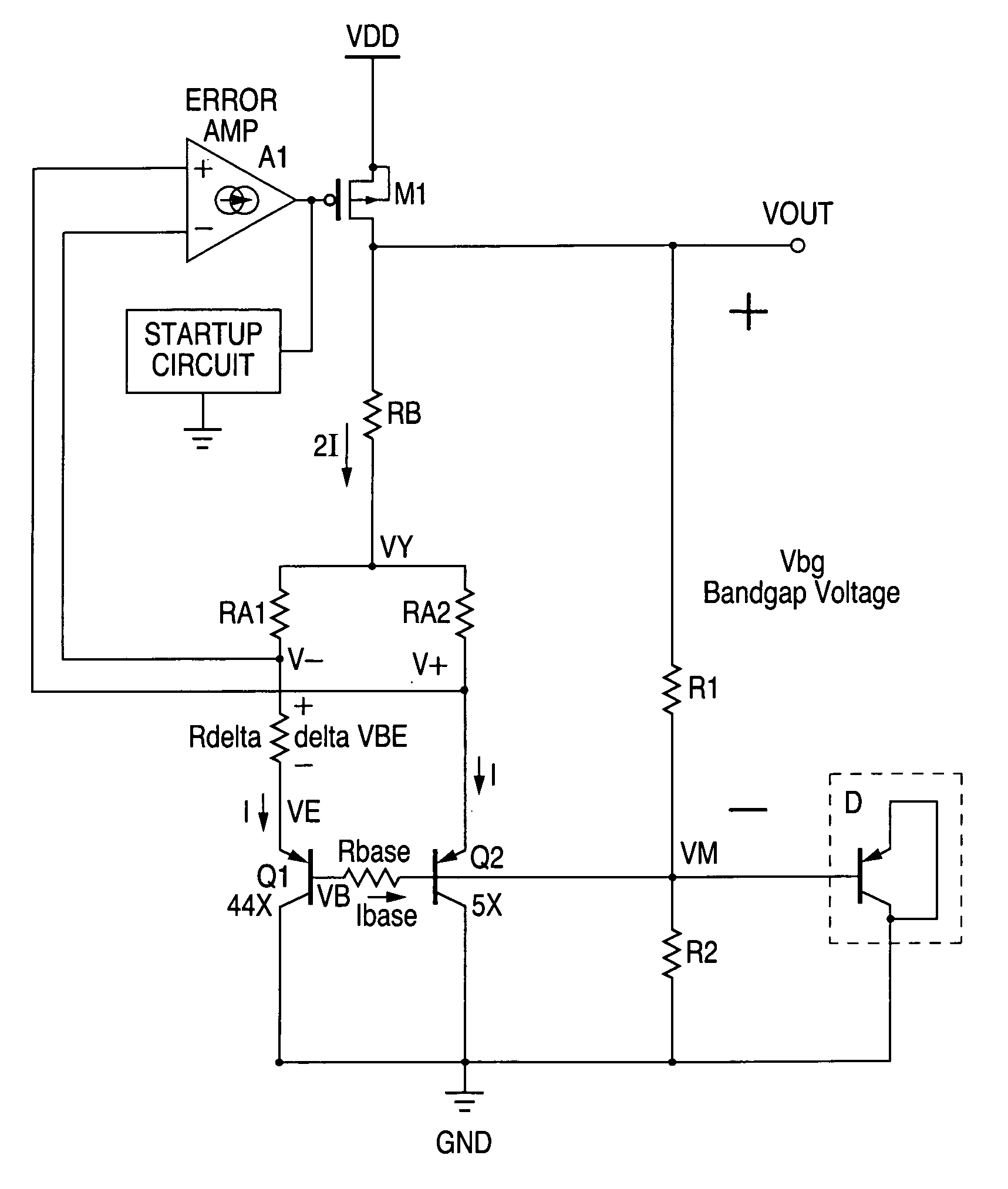
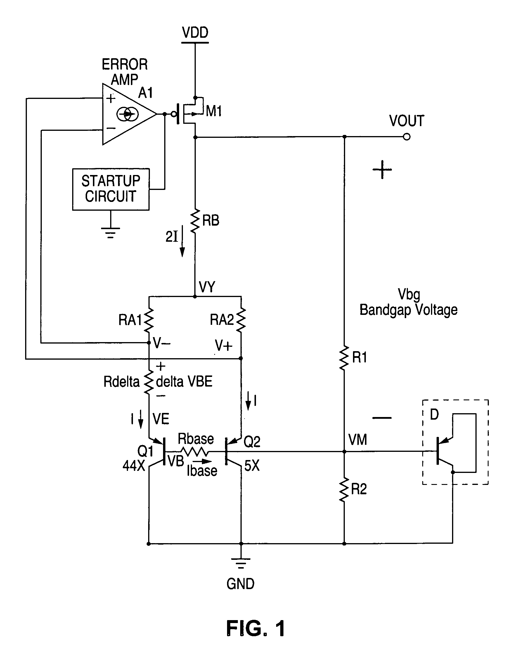
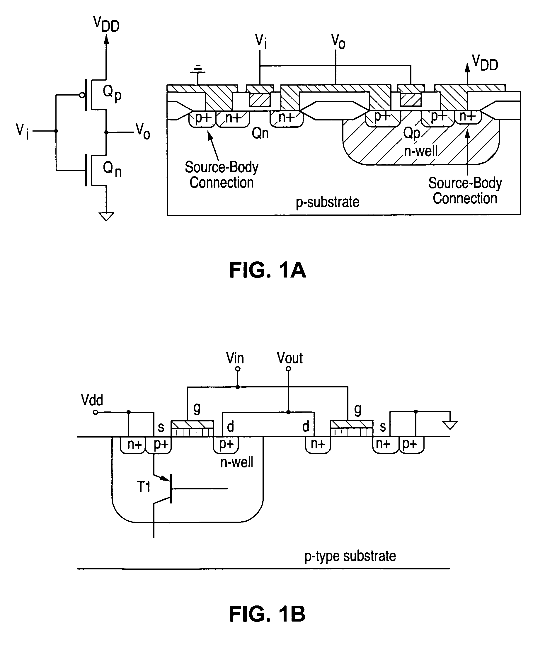
[0014]The following detailed description is of example embodiments of the presently claimed invention with references to the accompanying drawings. Such description is intended to be illustrative and not limiting with respect to the scope of the present invention. Such embodiments are described in sufficient detail to enable one of ordinary skill in the art to practice the subject invention, and it will be understood that other embodiments may be practiced with some variations without departing from the spirit or scope of the subject invention.

[0015]Throughout the present disclosure, absent a clear indication to the contrary from the context, it will be understood that individual circuit elements as described may be singular or plural in number. For example, the terms “circuit” and “circuitry” may include either a single component or a plurality of components, which are either active and / or passive and are connected or otherwise coupled together (e.g., as one or more integrated circ...


PUM


Abstract

A metal oxide semiconductor (MOS) bandgap voltage reference circuit with a plurality of dummy bipolar junction transistors (BJTs) coupled to the mismatched parasitic substrate BJTs for improving parasitic capacitance matching, thereby improving startup behavior of the bandgap reference circuitry.

Description

[0001]This is a continuation of U.S. patent application Ser. No. 10 / 730,201, filed on Dec. 5, 2003, now U.S. Pat. No. 6,858,917 and entitled “Metal Oxide Semiconductor (MOS) Bandgap Voltage Reference Circuit”.BACKGROUND OF THE INVENTION[0002]1. Field of the Invention[0003]The present invention relates to bandgap voltage generators, and in particular, to bandgap voltage generators using metal oxide semiconductor (MOS) devices.[0004]2. Description of the Related Art[0005]Bandgap voltage generator circuits are well known in the art and can be implemented using many circuit topologies. As is well known, the circuit relies on two transistors (generally implemented as two groups of mutually interconnected transistors) running at different emitter current densities, with the current-rich transistor typically running at ten or more times the density of the current-lean transistor. Such a factor of ten or more will cause a 60-millivolt difference between the base-emitter voltages Veb of the ...

Claims


Application Information

Patent Timeline
Patent Type & Authority Patents(United States)
IPC IPC(8): G05F3/08G05F3/30H01L27/085H01L27/07H01L27/092
CPCG05F3/30H01L27/0705H01L27/0921
Inventor RANUCCI, PAUL DAVID
Owner NAT SEMICON CORP
Why Eureka
Try Eureka