
Methods for patterning using liquid embossing

a technology of liquid embossing and patterning, applied in the field of patterning surfaces or layers, can solve the problems of limited resists or photoactivated polymers that can be used to form mask structures

Inactive Publication Date: 2005-08-30
KOVIO
View PDF76 Cites 103 Cited by
  • Summary
  • Abstract
  • Description
  • Claims
  • Application Information

AI Technical Summary

Benefits of technology

[0005]The current invention is directed to a method of patterning using a mask. As used herein, a mask means a patterned layer that is used in a subsequent step to pattern a layer above or below the mask. In accordance with the present invention, device layers are patterned using a mask, wherein the...

Problems solved by technology

Further, the materials that can be used to form the mask structure are limited to resists or photo-activated polymers.

Method used


Image

  • Methods for patterning using liquid embossing
  • Methods for patterning using liquid embossing
  • Methods for patterning using liquid embossing

Examples


Embodiment Construction

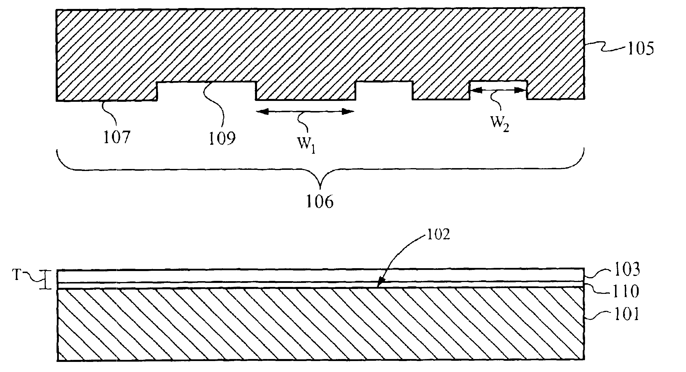
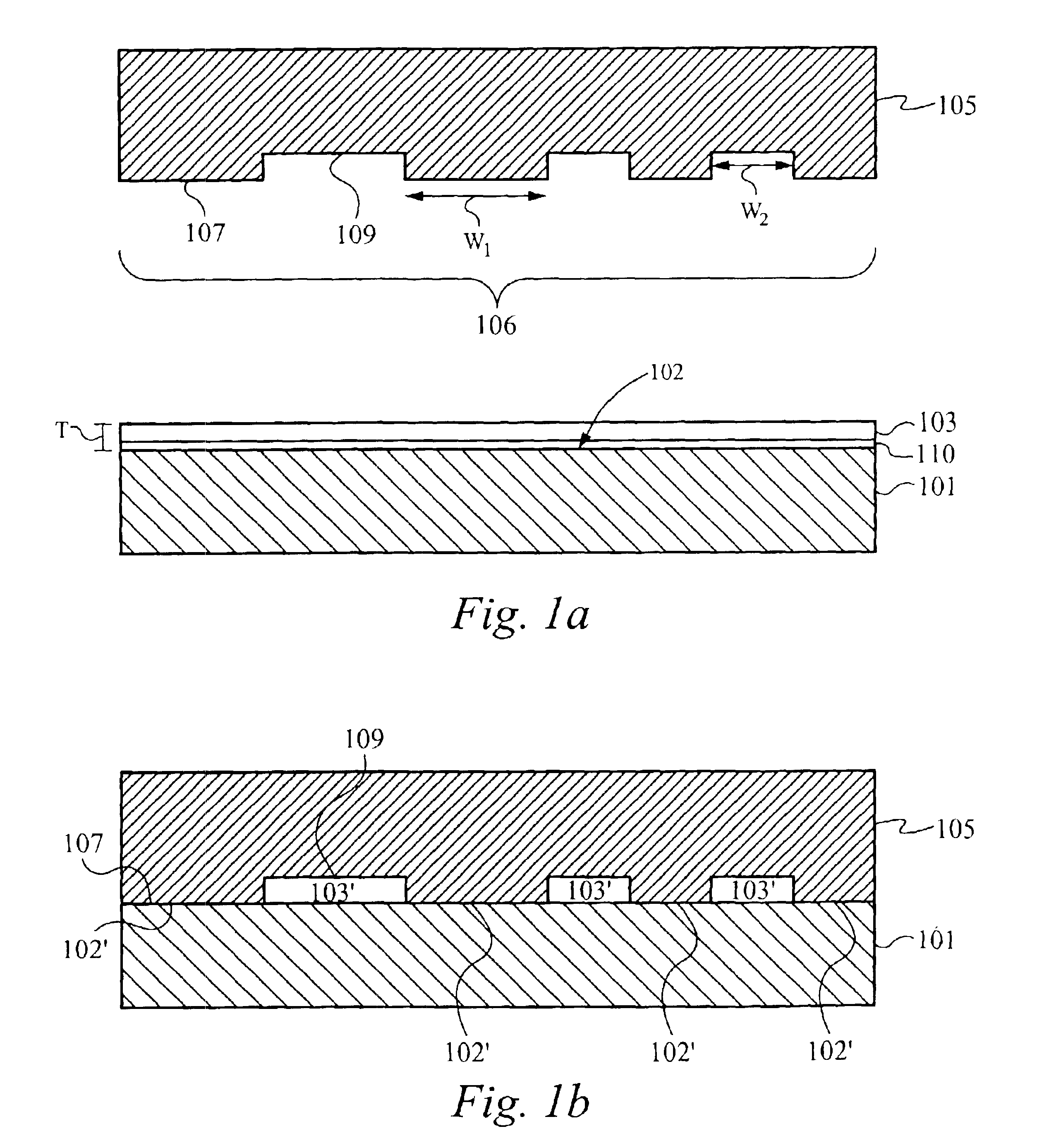
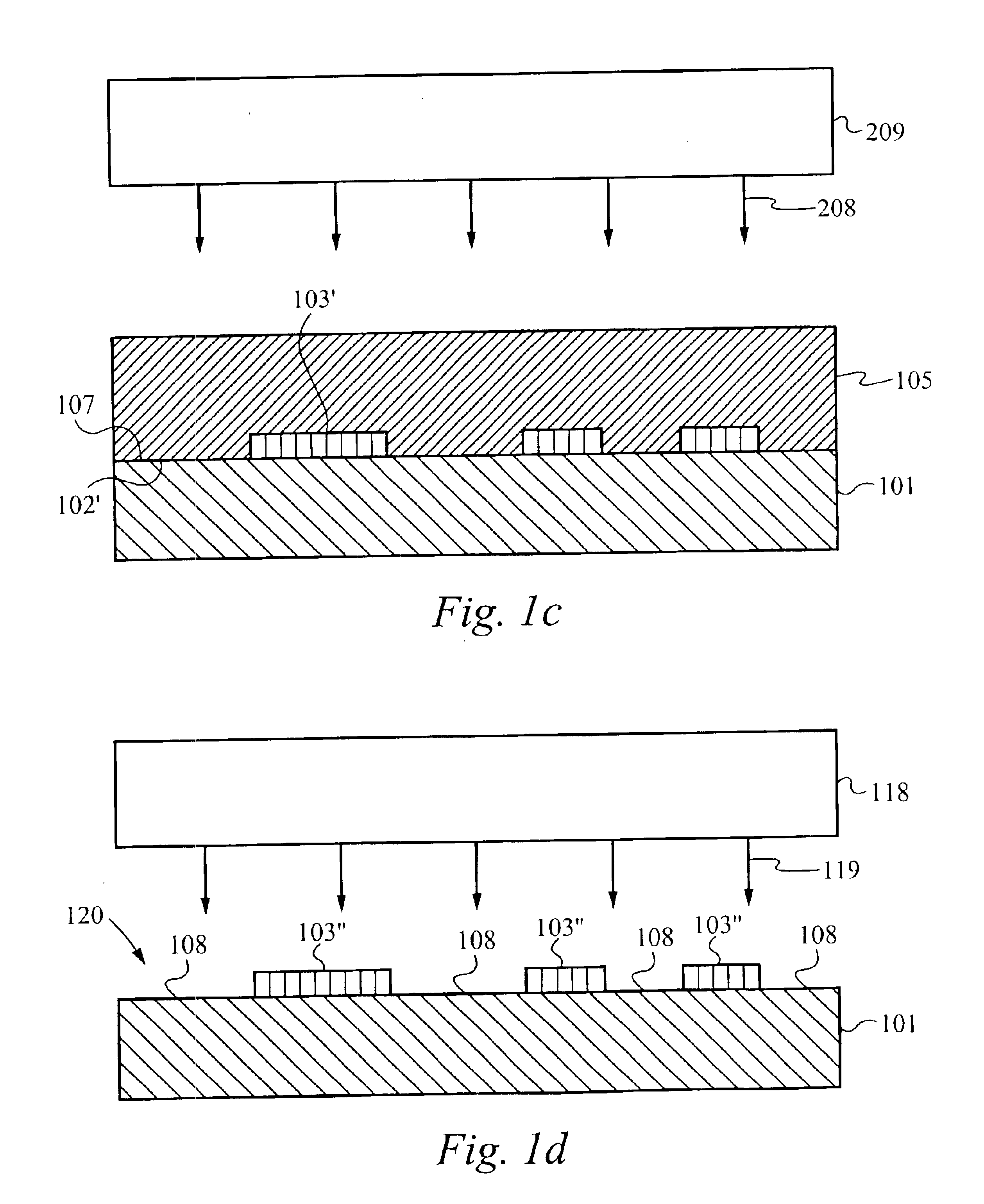
[0025]FIGS. 1A-D illustrate cross-sectional views of a micro-stamp 105 and a method of using the micro-stamp 105 to form a first patterned layer or mask structure, in accordance with the present invention. Referring to FIG. 1A, the micro-stamp 105 comprises an embossing surface 106 patterned with raised stamp features 107 and recessed stamp features 109. Preferably, a portion of the stamp features 107 and 109 are patterned to have lateral dimensions W1 and W2 in a range of 100 nanometers to 100 microns depending the application at hand. The stamp features 107 and 109 can be patterned to have lateral dimensions W1 and W2 as small as several tens of nanometers. Preferably, the micro-stamp 105 is formed from polydimethylsiloxane (PDMS), but it may be formed from other materials, including, but not limited to, silicon, metal, glass, quartz, rubber, or plastic.

[0026]FIG. 1A also illustrates a substrate 101 having a surface 102; an interface layer 110 formed over the surface 102; and a la...


PUM

PropertyMeasurementUnit
Polymericaaaaaaaaaa

Abstract

The current invention is directed to a method of patterning a surface or layer in the fabrication of a micro-device. In accordance with a preferred embodiment of the invention, a first mask structure is formed by depositing a layer of a first material onto the surface or layer and embossing the layer with a micro-stamp structure. The layer is preferably embossed as a liquid, which is solidified or cured to form the first mask structure. The first mask structure can be used as an etch-stop mask which is removed in a subsequent processing step or, alternatively, the first mask structure can remain a functional layer of the micro-device. In further embodiments, unmasked regions of the surface or layer are chemically treated through the first mask structure and / or a second material is deposited onto the unmasked regions of the surface or layer through the first mask structure to form a second mask structure and / or a second functional layer of the micro-device.

Description

RELATED APPLICATION(S)[0001]This patent application claims priority under 35 U.S.C. 119(e) of the co-pending U.S. Provisional Patent Application Ser. No. 60 / 328,591, filed Oct. 11, 2001, and titled “MICRO-STENCIL.” The Provisional Patent Application Ser. No. 60 / 328,591, filed Oct. 11, 2001, and titled “MICRO-STENCIL” is also hereby incorporated by reference.FIELD OF THE INVENTION[0002]The present invention relates to patterning surfaces or layers. More specifically, this invention relates to patterning surfaces or layers for the fabrication of micro-devices.BACKGROUND OF THE INVENTION[0003]Micro-mechanical, micro-electrical, and micro-optical devices are most typically fabricated using multiple mask and etching steps, which are fundamental steps in most photo-lithography processes. The etch-mask is typically formed by depositing a continuous layer of a photoresist polymer on a surface or layer, such as on a silicon wafer, to be patterned. The photoresist layer is selectively exposed...

Claims


Application Information

Patent Timeline
IPC IPC(8): B29C43/02B41M3/00B81C1/00G03F7/00B41M1/24B41M1/00H01L51/40H01L51/05
CPCB29C43/021B41M3/006B81C1/0046B82Y10/00B82Y40/00G03F7/0002B29C2043/023B41M1/24B81C2201/036H01L51/0004H10K71/13
Inventor BULTHAUP, COLINSPINDT, CHRIS
Owner KOVIO
Learn More