Thin-film electronic device module

a technology of electronic devices and thin films, applied in the direction of photomechanical devices, instruments, radio-controlled devices, etc., can solve the problems of reducing display resolution and size, increasing resistive heating power loss in traces, and consuming less power, so as to reduce power consumption, reduce power consumption, and increase reliability

Inactive Publication Date: 2005-08-30
OSRAM OLED
View PDF5 Cites 35 Cited by
  • Summary
  • Abstract
  • Description
  • Claims
  • Application Information

AI Technical Summary

Benefits of technology

[0011]An embodiment of an encapsulated electronic thin-film device is described that, for example, occupies less space on the substrate, has increased reliability, consumes less power, allows a connector to easily bond to the device, and allows a connector to be attached prior to substrate singulation. The embodiment of the encapsulated electronic thin-film device includes a substrate and an active area that is on the substrate. The active area includes at least one electronic thin-film element. The encapsulated electronic thin-film device also includes a thin-film encapsulation layer that covers at least the active area and this thin-film encapsulation layer is selectively deposited. The device further includes multiple conducting traces that are coupled to the active area. The multiple conducting traces protrude slightly past a perimeter of the thin-film encapsulation layer.

Problems solved by technology

Having a fine pitch between traces increases the resistance of the traces and thus higher voltage drivers are used resulting in greater power consumption and increased resistive heating power loss in the traces.
The increase in resistance and voltage results in fewer number of traces being used in the display and hence the number of rows and columns are reduced resulting in reduced display resolution and size.
Having a fine pitch between traces increases the likelihood that one trace will electrically short another trace.
In addition, the fine pitch can cause electrochemical reactions or electromigration that also increases the likelihood of an electrical short.
If the number of displays per mother glass is reduced, then the cost per display increases.
The increase in the space occupied due to routing the traces to only one side and due to the perimeter seal 112 results in reduced design freedom.

Method used


Image

  • Thin-film electronic device module
  • Thin-film electronic device module
  • Thin-film electronic device module

Examples


first embodiment

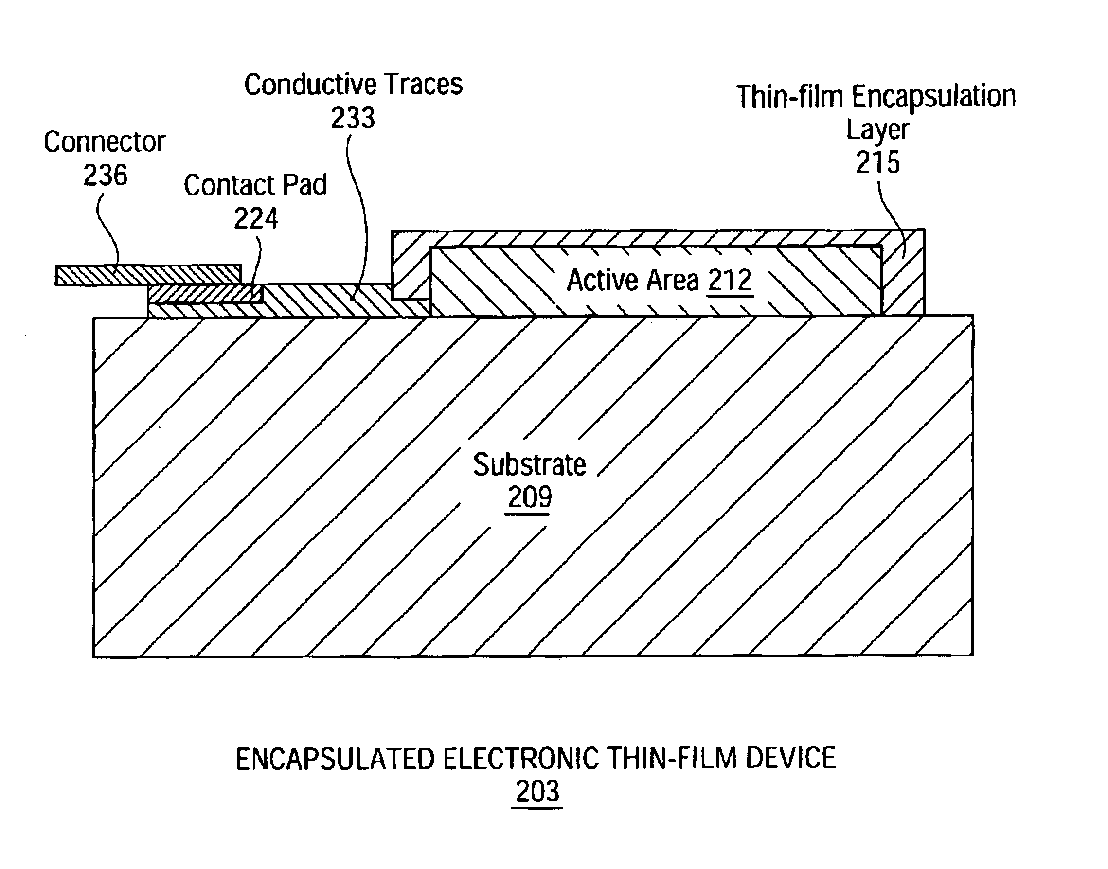
[0026]FIG. 4 shows an encapsulated electronic thin-film device according to the present invention. An encapsulated electronic thin-film device 203 includes an active area 212 on a substrate 209. As used within the specification and the claims, the term “on” includes when there is direct physical contact between the two parts and when there is indirect contact between the two parts because they are separated by one or more intervening parts. The active area 212 is comprised of one or more electronic thin-film elements 221. The one or more electronic thin-film elements 221 is formed at the one or more intersections between the one or more row electrodes and the one or more column electrodes in which the one or more row electrodes are perpendicular to the one or more column electrodes and a semiconductive material is between those two electrodes. One end of the conductive traces 233 is coupled to the one or more row electrodes and one end of the conductive traces 230 is coupled to the ...

second embodiment

[0037]FIG. 8a shows an encapsulated electronic thin-film device according to the present invention. An encapsulated electronic thin-film device 403 includes the active area 212 on the substrate 209. The active area 212 is comprised of one or more of the electronic thin-film elements 221. The thin-film encapsulation layer 215 is selectively deposited on at least the active area 212 to cover at least the active area 212. The thickness of the thin-film encapsulation layer 215 is, for example, less than about 200 micrometers thick, preferably less than about 100 micrometers thick, more preferably less than about 50 micrometers thick. In the configuration shown in FIG. 8a, the thin-film encapsulation layer 215 extends slightly past the perimeter of the active area 212. The range of this slight extension is, for example, from about 10 um to about 10 mm, and preferably from about 0.5 mm to about 3 mm. In another configuration (not shown), the thin-film encapsulation layer 215 may only cove...

fourth embodiment

[0038]FIG. 8b shows a connector according to the present invention. In this embodiment, a connector 440 includes connector traces 443, connector traces 446, and connector traces 449. The connector traces 443 are coupled to the contact pad 415, the connector traces 446 are coupled to the contact pad 421, and the connector traces 449 are coupled to the contact pad 427. Here, the connector 440 covers all of the active area 212. In one configuration of this embodiment, each of the row electrodes of the active area 212 is coupled to a particular one of the conductive traces 412 and also a particular one of the conductive traces 424 and thus to the contact pad 415 and the contact pad 427 respectively. Coupling each of the row electrodes to both the contact pads reduces the voltage drops along the rows inside the active area 212. In another configuration, the conductive traces 412 and the conductive traces 424 are each coupled to only half of the row electrodes. For example, the conductive...


PUM


Abstract

In an embodiment of this invention, an encapsulated electronic thin-film device includes a substrate and an active area is fabricated on the substrate. The active area is comprised of at least one electronic thin-film element. A thin-film encapsulation layer is selectively deposited on at least the active area to cover at least the active area. Traces protrude slightly past a perimeter of the thin-film encapsulation layer. The traces are routed to two or more contact pads to which one or more connectors can attach. Attaching the connector to the contact pads allows an external device to be coupled to the active area of the electronic thin-film device.

Description

BACKGROUND OF THE INVENTION[0001]An electronic thin-film device is typically encapsulated to protect it from, for example, moisture and / or oxygen in order to prevent or reduce degradation and device failure. The device contains multiple elements and these elements are typically connected to external devices. In order to connect to external devices, traces from the elements are routed to the perimeter of the electronic thin-film device where these traces are connected to the external device using, for example, one or more flex connectors, a printed circuit board (“PCB”), or a chip-on glass driver.[0002]Examples of the electronic thin-film device are: an active or passive matrix OLED display, an active or passive matrix OLED light source, an active or passive matrix inorganic electroluminescent display, an organic or inorganic detector array, an organic or inorganic solar cell array, or an organic or inorganic thin-film transistor array. These devices are know in the art and are discu...

Claims


Application Information

Patent Timeline
Patent Type & Authority Patents(United States)
IPC IPC(8): H01L23/28H01L31/0203H01L27/144H01L27/32H01L51/52
CPCH01L27/3276H01L27/3288H01L51/5253H01L27/1446H10K59/179H10K59/131H10K50/844
Inventor PICHLER, KARL
Owner OSRAM OLED
Why Eureka
Try Eureka