Alignment mark and alignment method using the same for photolithography to eliminating process bias error

a technology of alignment mark and alignment method, which is applied in the direction of photomechanical treatment, semiconductor devices, instruments, etc., can solve the problems of increasing the complexity of integrated circuit design, increasing the alignment accuracy requirement of each layer of circuit pattern, and increasing the critical dimension of integrated circui

Inactive Publication Date: 2005-08-30
PROMOS TECH INC
View PDF2 Cites 19 Cited by
  • Summary
  • Abstract
  • Description
  • Claims
  • Application Information

AI Technical Summary

Benefits of technology

[0007]In one aspect, the present invention provides an alignment method for eliminating process bias error to fix the position of an alignment target.
[0008]In another aspect, the present invention provides an alignment method for eliminating process bias error. When a thin film, having an asymmetrical profile, is deposited on an alignment mark, the position of an alignment target is not changed by the film deposition.
[0009]In still another aspect, the present invention provides an alignment method for eliminating process bias error to increase alignment accuracy for aligning each layer of circuit pattern.

Problems solved by technology

The complexity of integrated circuit design increases as the integration of the integrated circuit increases, and the critical dimension of the integrated circuit is continually reduced.
Since the integrated circuit is formed by overlapping multiple layers of circuit patterns, the alignment accuracy requirement of each layer of circuit pattern is continually higher and harder to achieve.
In particular, the gravity of the alignment accuracy problem is increased when a thin film on alignment marks has an asymmetrical profile, which usually results from asymmetrically depositing the thin film or chemical mechanical polishing the thin film.
Thus, an alignment bias error occurs.
Therefore, similar problems are also encountered.

Method used


Image

  • Alignment mark and alignment method using the same for photolithography to eliminating process bias error
  • Alignment mark and alignment method using the same for photolithography to eliminating process bias error
  • Alignment mark and alignment method using the same for photolithography to eliminating process bias error

Examples


Embodiment Construction

[0025]Reference will now be made in detail to the present preferred embodiments of the invention, examples of which are illustrated in the accompanying drawings.

[0026]For solving the problems encountered by the prior arts, i.e. the alignment bias error produced by the asymmetrical profile of a thin film formed on alignment marks, the present invention provides an alignment mark and a photolithography alignment method using the same for eliminating process bias error.

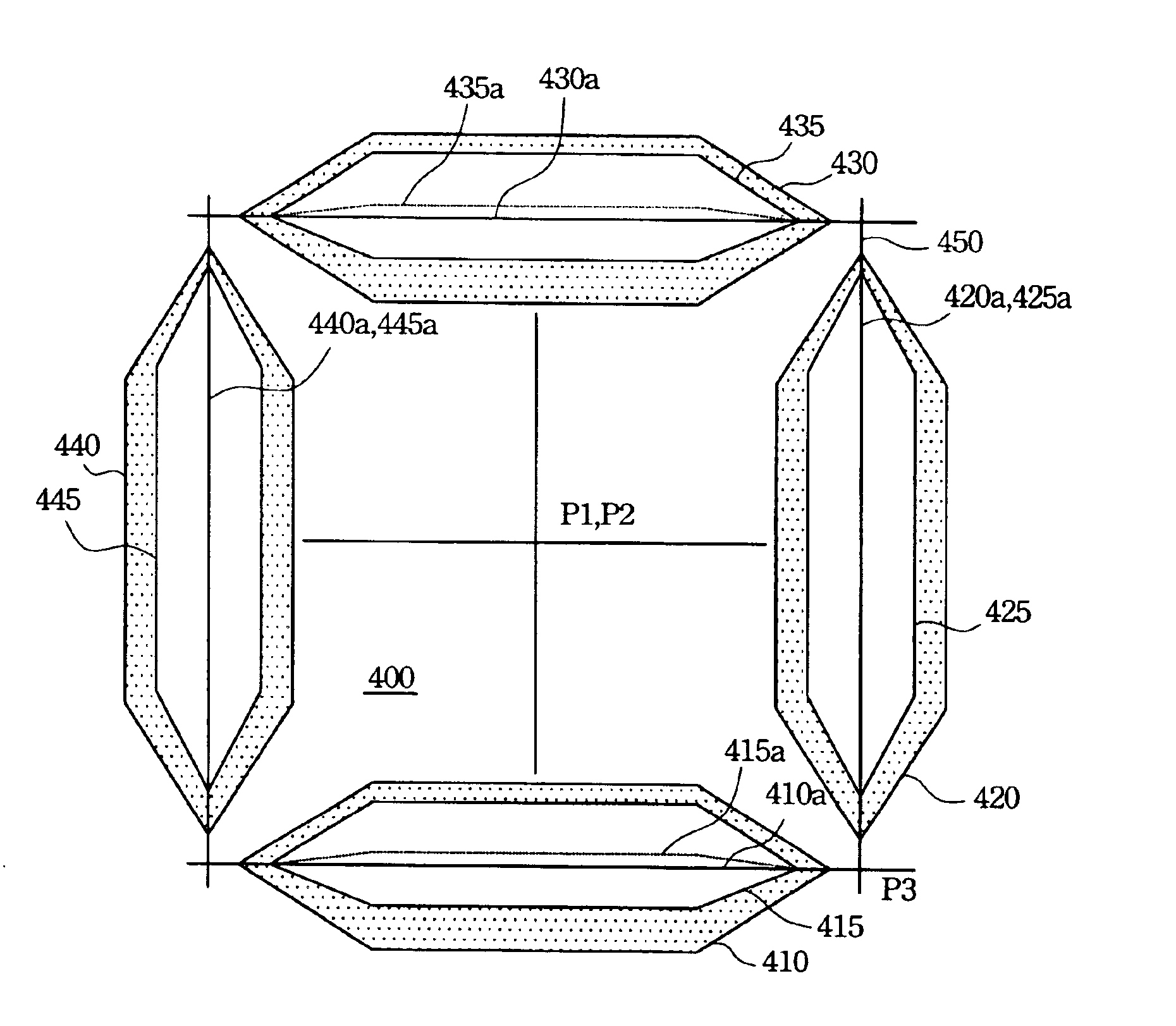
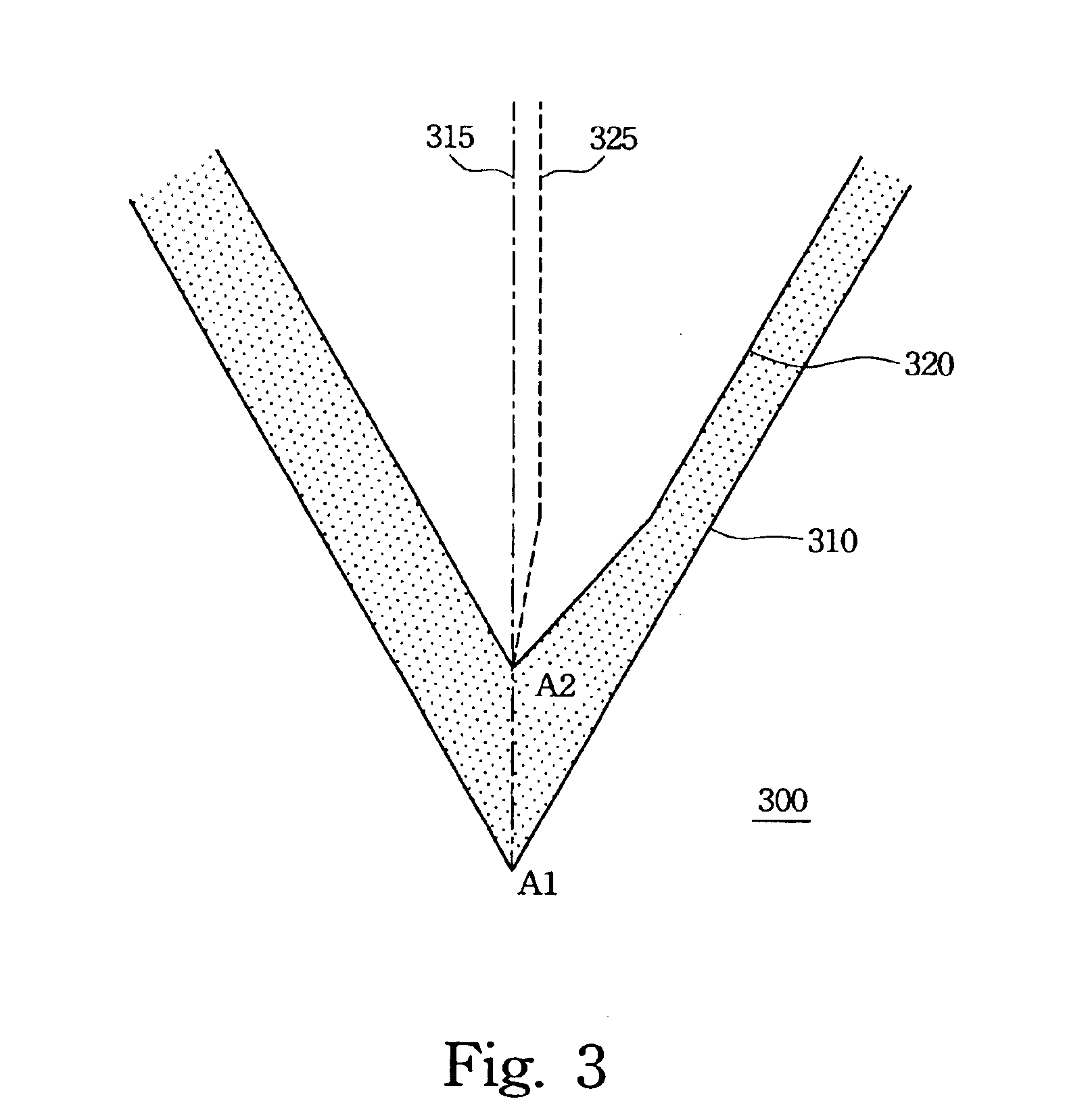
[0027]A partial enlarged top view of an alignment mark according to a preferred embodiment of the present invention is shown in FIG. 3. In FIG. 3, a trench 310 is formed on a substrate 300 to be an alignment mark. A film is subsequently formed on the substrate 300, and a trench 320 is simultaneously formed in the trench 310. An asymmetrical profile of the thin film in the trench 310 can be produced by various process bias errors. Hence, the centerline 325 of the trench 320 and the centerline 315 of the trench 310 are not...


PUM

PropertyMeasurementUnit
depthaaaaaaaaaa
shapeaaaaaaaaaa
areaaaaaaaaaaa

Abstract

An alignment mark is made of at least two nonparallel trenches having two reducing-width-to-zero ends. The displacement bias error, produced by a process bias error, of the centerlines of the trenches is zero where the width of the two trenches is zero. Hence, the alignment target on a substrate can be reproduced.

Description

BACKGROUND OF THE INVENTION[0001]1. Field of Invention[0002]The present invention relates to a manufacturing process of semiconductor integrated circuit. More particularly, the present invention relates to an alignment mark and a photolithography alignment method using the same for eliminating process bias error.[0003]2. Description of Related Art[0004]The complexity of integrated circuit design increases as the integration of the integrated circuit increases, and the critical dimension of the integrated circuit is continually reduced. Since the integrated circuit is formed by overlapping multiple layers of circuit patterns, the alignment accuracy requirement of each layer of circuit pattern is continually higher and harder to achieve. In particular, the gravity of the alignment accuracy problem is increased when a thin film on alignment marks has an asymmetrical profile, which usually results from asymmetrically depositing the thin film or chemical mechanical polishing the thin fil...

Claims


Application Information

Patent Timeline
Patent Type & Authority Patents(United States)
IPC IPC(8): G03F9/00H01L23/544
CPCG03F9/7076G03F9/708G03F9/7084
Inventor CHIEN, TONY
Owner PROMOS TECH INC
Why Eureka
Try Eureka