Diagonal deep well region for routing body-bias voltage for MOSFETS in surface well regions

a surface well and mosfet technology, applied in semiconductor devices, semiconductor device details, instruments, etc., can solve the problems of wasting a large amount of time and resources, and generating the physical layout of a semiconductor device having mosfets (metal oxide semiconductor field effect transistors) formed on a semiconductor substra

Inactive Publication Date: 2005-08-30
DEEPWELL IP LLC
View PDF11 Cites 57 Cited by
  • Summary
  • Abstract
  • Description
  • Claims
  • Application Information

AI Technical Summary

Problems solved by technology

Generation of the physical layout of a semiconductor device having MOSFETS (metal oxide semiconductor field effect transistors) formed on a semiconductor substrate is a challenging task.
An extensive amount of time and resources are spent during the creation of the physical layout.
Unfortunately, this process of modifying the existing physical layout typically requires forming an additional routing layer for the body-bias voltage on the surface of the semiconductor device, creating a serious issue since the existing physical layout utilizes most, if not all, available surface area.

Method used


Image

  • Diagonal deep well region for routing body-bias voltage for MOSFETS in surface well regions
  • Diagonal deep well region for routing body-bias voltage for MOSFETS in surface well regions
  • Diagonal deep well region for routing body-bias voltage for MOSFETS in surface well regions

Examples


Embodiment Construction

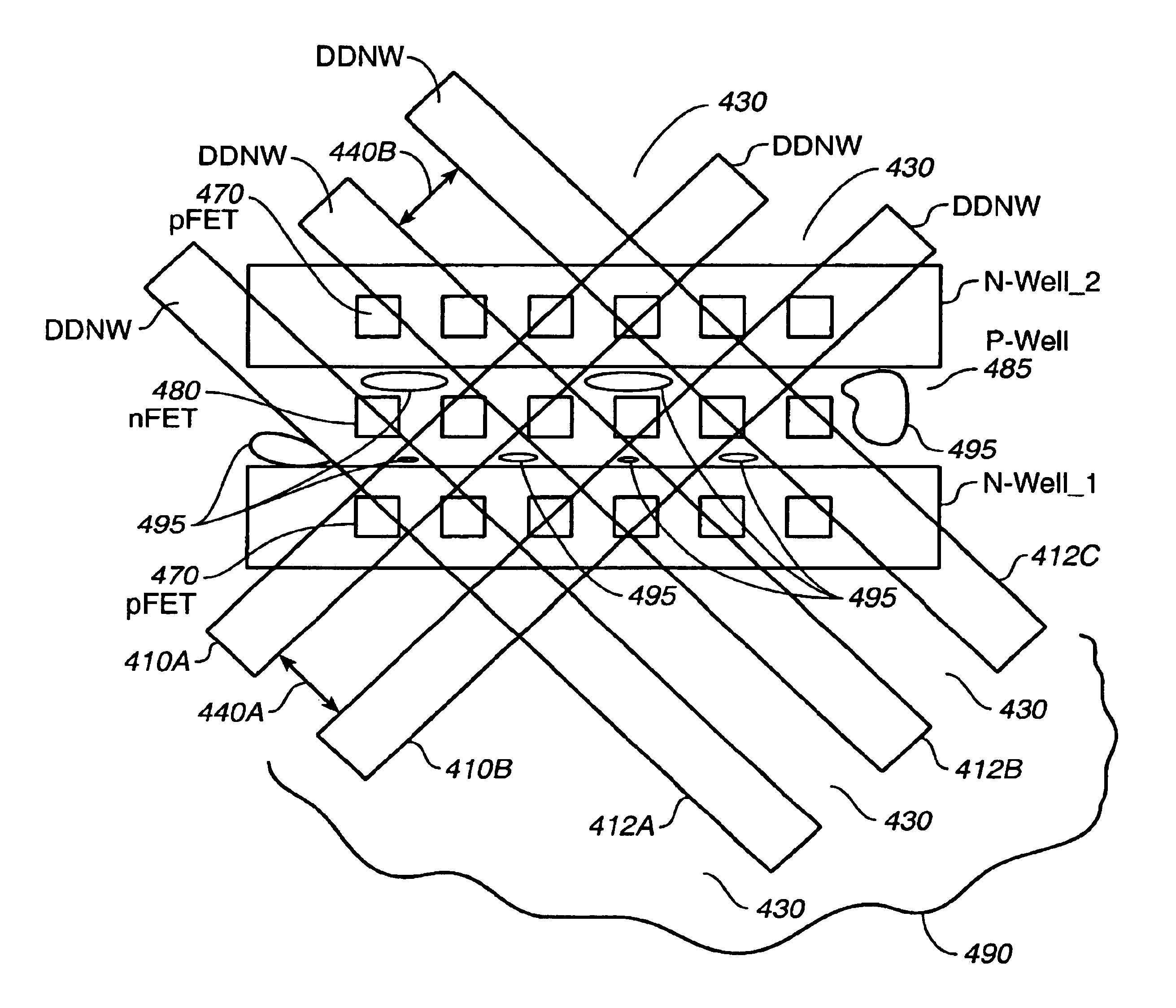
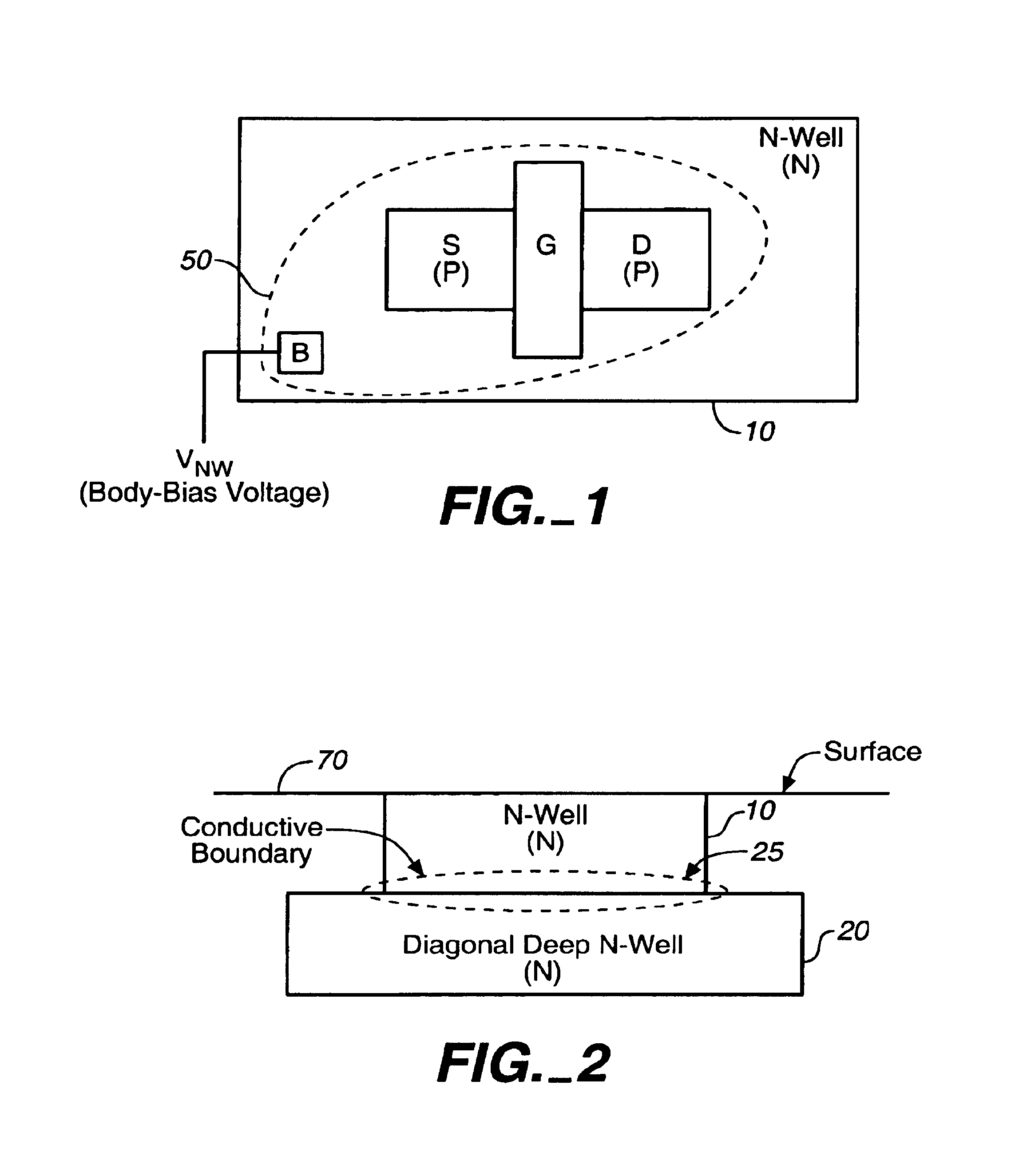
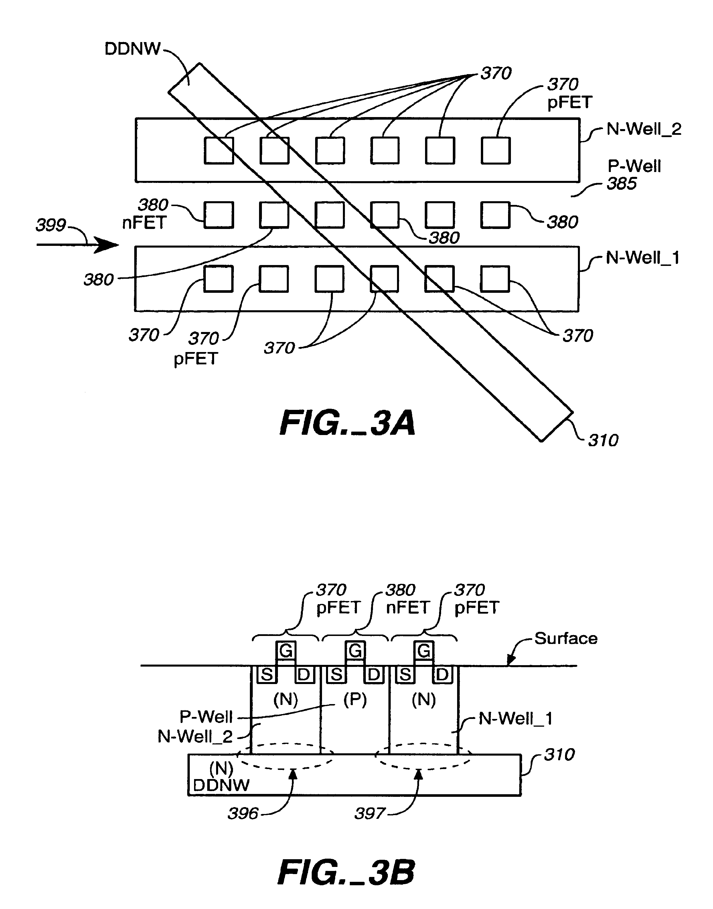
[0013]Reference will now be made in detail to the preferred embodiments of the present invention, examples of which are illustrated in the accompanying drawings. While the invention will be described in conjunction with the preferred embodiments, it will be understood that they are not intended to limit the invention to these embodiments. On the contrary, the invention is intended to cover alternatives, modifications and equivalents, which may be included within the spirit and scope of the invention as defined by the appended claims. Furthermore, in the following detailed description of the present invention, numerous specific details are set forth in order to provide a thorough understanding of the present invention. However, it will be recognized by one of ordinary skill in the art that the present invention may be practiced without these specific details.

[0014]Although the following description of the present invention will focus on routing a body-bias voltage to pFETS (or p-type...


PUM


Abstract

Diagonal deep well region for routing the body-bias voltage for MOSFETS in surface well regions is provided and described.

Description

BACKGROUND OF THE INVENTION[0001]1. Field of the Invention[0002]The present invention generally relates to MOSFETS (metal oxide semiconductor field effect transistors). More particularly, the present invention relates to the field of routing body-bias voltage to the MOSFETS.[0003]2. Related Art[0004]Generation of the physical layout of a semiconductor device having MOSFETS (metal oxide semiconductor field effect transistors) formed on a semiconductor substrate is a challenging task. An extensive amount of time and resources are spent during the creation of the physical layout. However, consumption of resources can be minimized if new physical layouts utilize substantial potions of existing physical layouts. For example, a new physical layout having MOSFETS that are body-biased would be less expensive to generate if an existing physical layout having MOSFETS without body-bias is utilized and modified according to the needs of the new physical design. Unfortunately, this process of mo...

Claims


Application Information

Patent Timeline
Patent Type & Authority Patents(United States)
IPC IPC(8): H01L21/70H01L21/8234H01L21/8238H01L27/085H01L27/02H01L27/092
CPCG11C5/146H01L21/823493H01L21/823892H01L27/0203H01L27/0222H01L27/0928H01L2924/0002H01L2924/00H01L23/481H01L29/0646H01L29/1095
Inventor PELHAM, MIKEBURR, JAMES B.
Owner DEEPWELL IP LLC
Why Eureka
Try Eureka