
Display, portable device, and substrate

a portable device and substrate technology, applied in static indicating devices, instruments, optics, etc., can solve the problems of not guaranteeing identical characteristics between neighboring fets, entail the time-ratio gray-scale method, and produce a homogeneous gray-scale display across the entire screen. , to achieve the effect of suppressing moving picture breakup

Inactive Publication Date: 2005-08-30
SHARP KK
View PDF31 Cites 111 Cited by
  • Summary
  • Abstract
  • Description
  • Claims
  • Application Information

AI Technical Summary

Benefits of technology

[0044]Consequently, with the arrangement in which each pixel has memory means (memory) and potential maintaining means (capacitor), more tones than memories provided to the pixels can be displayed. Further, by switching between the memories provided to the pixels, a video image is switchably selected to produce a display without externally receiving further data. Moreover, the first memory element can be caused to retain a voltage corresponding to the largest tone data, a voltage application time for that data can be divided in the application of voltage, so as to suppress moving picture breakups.

Problems solved by technology

The structure including a current mirror circuit requires its components, the FETs 223, 224, to have identical characteristics; however, fabricating the FETs by a polysilicon process, which is used for fabrication of liquid crystal displays for example, does not guarantee identical characteristics between neighboring FETs.
As a result, the circuit for an analog gray-scale method in FIG. 26 entails a problem of irregular characteristics in polysilicon TFTs and can produce a homogeneous gray-scale display across the entire screen only with difficulties.
However, the time-ratio gray-scale method could probably entail the development of moving picture breakup (dynamic false contours) as is the case with PDPs (plasma display panels).
This is not easy even with a present low-temperature polysilicon process.
When this is the case, the device can produce a maximum of only 8 tones and lacks appeal as a commercial product.
Nevertheless, locating the memory outside the display region requires an additional area on the display substrate, which means a smaller number of substrates fabricated from a glass substrate (of an equal display area) in a TFT process and an increased manufacturing cost for a substrate of an equal display area.
However, the above technique is not still preferable in the portable device market where miniaturization and light weight are the key factors, since a larger substrate size is required to produce an equal display area.

Method used


Image

  • Display, portable device, and substrate
  • Display, portable device, and substrate
  • Display, portable device, and substrate

Examples


embodiment 1

[Embodiment 1]

[0081]The following will describe an embodiment in accordance with the present invention in reference to FIG. 1.

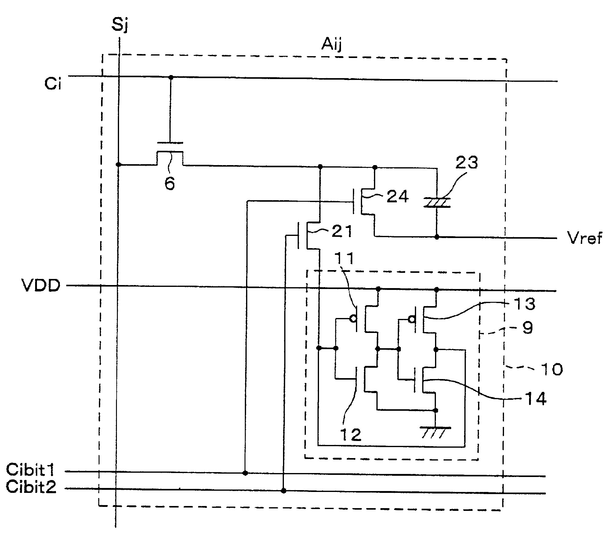
[0082]FIG. 1 shows an equivalent circuit of a pixel Aij which is a first arrangement of first means in accordance with the present invention. The equivalent circuit is adapted so that a data wire Sj, as a signal line, is connected to the source terminal of a TFT (thin film transistor, first switching means) 6 and that the source terminal of a TFT (second switching element) 21 and a pixel electrode of a liquid crystal element (electro-optic element) 23 which doubles as potential maintaining means are connected to the drain terminal of the TFT 6. A memory circuit (first memory element) 9, which is a static memory element, is connected to the drain terminal of the TFT 21.

[0083]The TFT 6 is needed, because the data wire Sj does not make a one-to-one correspondence to the electro-optic element. If the data wire Sj is arranged to make such a correspondence to the e...

embodiment 2

[Embodiment 2]

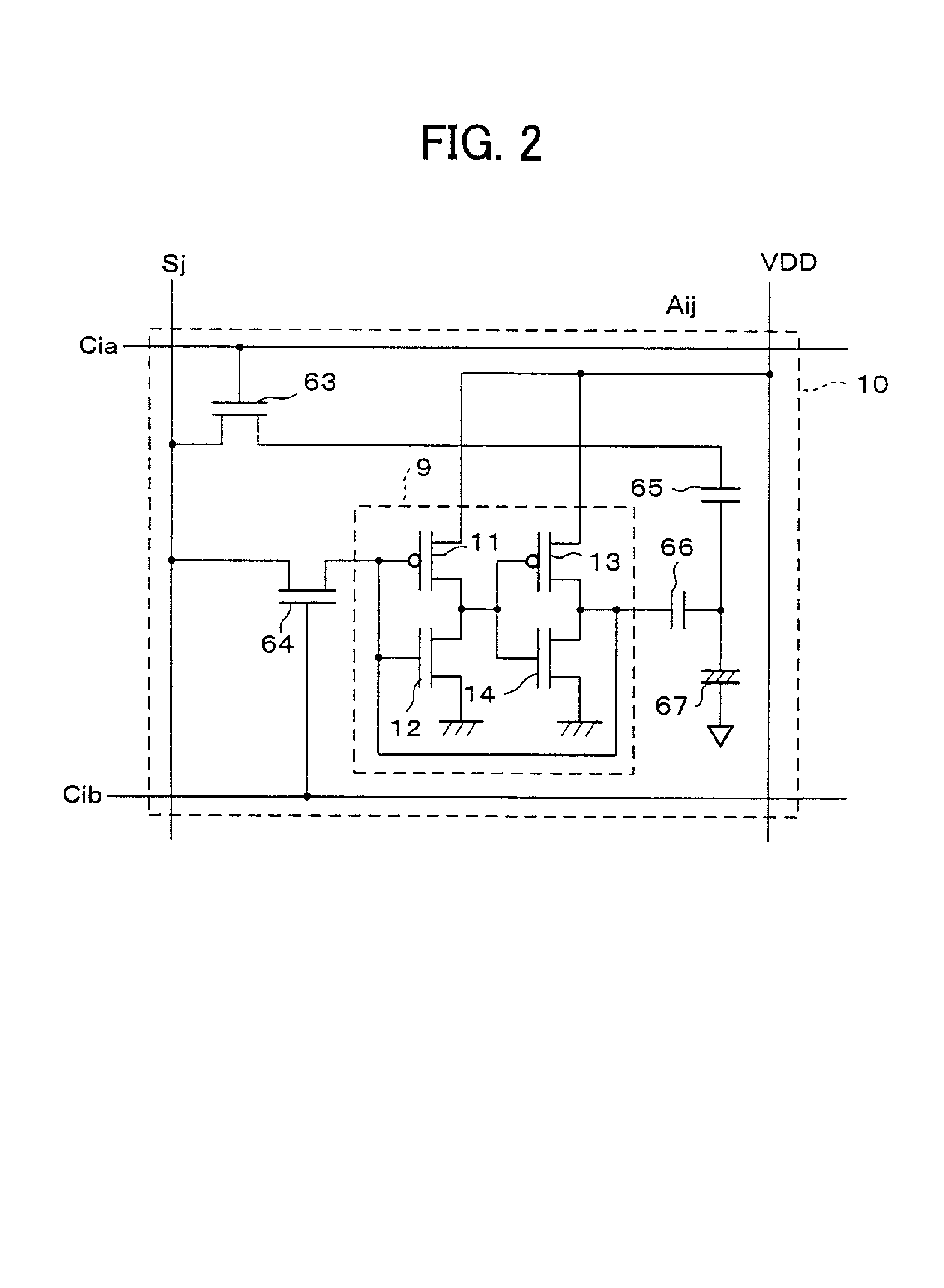
[0099]FIG. 2 shows an equivalent circuit of a pixel Aij which is a second arrangement of the first means in accordance with the present invention. The equivalent circuit includes a TFT (first switching means) 63 so that a data wire Sj, as a signal line, is connected to the source terminal of the TFT 63 and that a capacitor (potential maintaining means) 65 is connected to the drain terminal of the TFT 63. The equivalent circuit further includes a TFT (fourth switching means) 64 so that a data wire Sj, as a signal line, is connected to the source terminal of the TFT 64 and that an input terminal of a memory element (memory means) 9 is connected to the drain terminal of the TFT 64. A scan line Cia is connected to the gate terminal of the TFT 63, and a scan line Cib is connected to the gate terminal of the TFT 64.

[0100]This memory element 9 is identical to that in FIG. 1 and has a static memory structure in which an inverter formed by a p-type TFT 11 and an n-type TFT 12 i...

embodiment 3

[Embodiment 3]

[0105]FIG. 3 shows an equivalent circuit of a pixel Aij which is a second arrangement of first means in accordance with the present invention. The equivalent circuit is adapted so that a data wire Sj, as a signal line, is connected to the source terminal of a TFT (first switching means) 63, that an input terminal of a static memory (potential maintaining means) 68 is connected to the drain terminal of the TFT 63, that a data wire Sj, as a signal line, is connected to the source terminal of a TFT (fourth switching means) 64, and that the input terminal of a static memory (memory means) 69 is connected to the drain terminal of the TFT 64. A scan line Cia is connected to the gate terminal of the TFT 63, and a scan line Cib is connected to the gate terminal of the TFT 64.

[0106]An output terminal of the potential maintaining means 68 is connected to the source terminal of a p-type TFT (fifth switching element) 70, and the drain terminal of the TFT 70 is connected to a gate ...


PUM

PropertyMeasurementUnit
voltage amplitudeaaaaaaaaaa
gate voltageaaaaaaaaaa

Abstract

A memory circuit is caused to retain a voltage corresponding to largest tone data, then a voltage corresponding to tone data except for the largest tone data is applied to a liquid crystal element, and the voltage corresponding to the largest tone data is supplied from the memory circuit to the liquid crystal element. The development of moving picture breakups can be suppressed with a display producing a time-division gray-scale display, without having to carry out a display scanning operation for every display.

Description

FIELD OF THE INVENTION[0001]The present invention relates to displays, portable devices, and substrates in or on which every pixel has a memory element and a light-emitting element.BACKGROUND OF THE INVENTION[0002]The organic LED (light-emitting diode) display, a type of flat panel display, is a recent focus of attention as a competitor of the liquid crystal display. A great deal of efforts are put into the development of display circuits and driving methods for the organic LED display.[0003]Drive circuits and methods for use with the organic LED display are divided into two major categories: passive and active. To apply the active drive technology to organic LED displays, those TFT which drive the pixels have to be made of polysilicon.[0004]This is because when self-luminous elements are to be driven by TFTs as in the organic LED display, sufficient movement is required with electric charges in the silicon forming the TFTs to ensure an amount of current flow through the self-lumino...

Claims


Application Information

Patent Timeline
Patent Type & Authority Patents(United States)
IPC IPC(8): G09G3/36G09G3/32G09G3/00H05B33/02H05B33/08G02F1/133G09G3/20H05B44/00
CPCG09G3/3258G09G3/3648G09G3/3659G09G3/2011G09G3/2022G09G2300/0814G09G2300/0828G09G2300/0838G09G2300/0857G09G2310/0262G09G2310/061G09G2320/0261G02F1/133
Inventor NUMAO, TAKAJI
Owner SHARP KK
Features
  • Generate Ideas
  • Intellectual Property
  • Life Sciences
  • Materials
  • Tech Scout
  • Unparalleled Data Quality
  • Higher Quality Content
  • 60% Fewer Hallucinations
Learn More