Method and apparatus for amplitude filtering in the frequency plane of a lithographic projection system

a technology of lithographic projection system and frequency plane, which is applied in the direction of photomechanical treatment, printing, instruments, etc., can solve the problems of affecting the optical performance of scanning tools, affecting the filtering of tools, and undesirable aberrations, so as to achieve the effect of increasing the resolution of images

Inactive Publication Date: 2005-09-06
QIMONDA +1
View PDF3 Cites 27 Cited by
  • Summary
  • Abstract
  • Description
  • Claims
  • Application Information

AI Technical Summary

Benefits of technology

[0004]Bearing in mind the problems and deficiencies of the prior art, it is an object of the present invention to provide a method and apparatus for projecting a mask pattern image in a photolithography tool which increases resolution of the image, without resorting to a phase shifting mask.
[0005]It is another object to provide a method and apparatus of modifying the amplitude of a selected diffracted order of a mask pattern without causing a heating of the area in the vicinity of the projection lens system.
[0006]It is another object to provide a method and apparatus for preventing a selected order of the energy of the projected mask pattern image beam from reaching the image plane of the substrate.
[0011]Preferably, the optical element is adapted to deflect the zeroth order beams of the projected mask pattern, and permit higher order beams of the mask pattern to reach the image plane and form the projected pattern on the substrate. More preferably, the optical element is a diffractive element adapted to diffract zeroth order beams of the projected pattern at an obtuse angle. The diffractive element diffracts zeroth order beams of the projected mask pattern image without heating surrounding optical material through which beams of the projected mask pattern image pass and changing index of refraction of the optical material to an extent that affects the projected mask pattern image.

Problems solved by technology

However, introduction of the filter in tools has been hindered by the fact that an opaque filter absorbs energy and gets heated.
The result of this is that the surrounding optical materials, such as glass, through which the light passes are heated to such an extent that the index of refraction is changed sufficiently to affect the imaging characteristics of the projection system, causing undesirable aberrations.
Thus, there is a considerable problem in jeopardizing the optical performance of the scanning tool which projects the mask pattern image onto the wafer substrate.

Method used


Image

  • Method and apparatus for amplitude filtering in the frequency plane of a lithographic projection system
  • Method and apparatus for amplitude filtering in the frequency plane of a lithographic projection system
  • Method and apparatus for amplitude filtering in the frequency plane of a lithographic projection system

Examples


Embodiment Construction

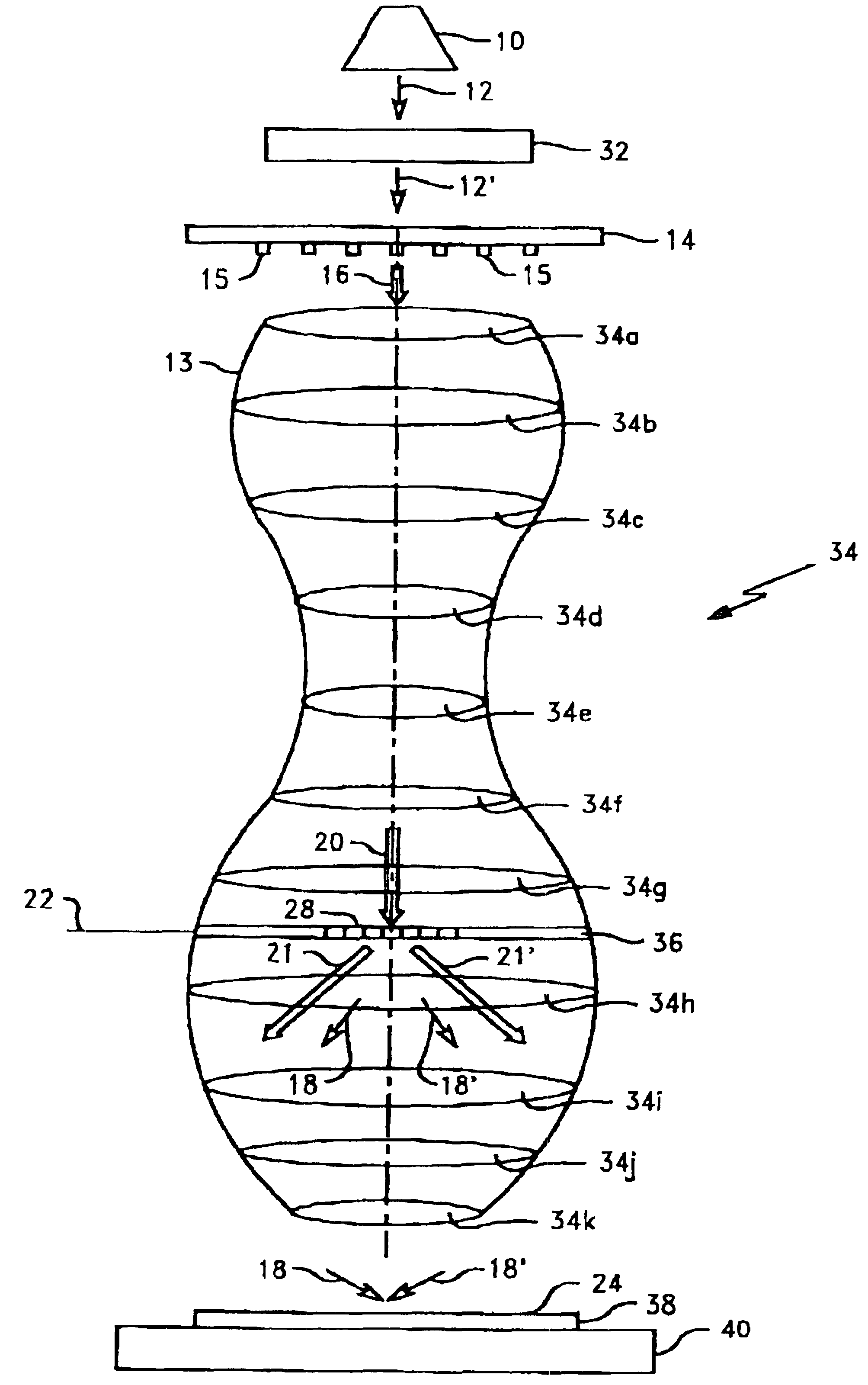
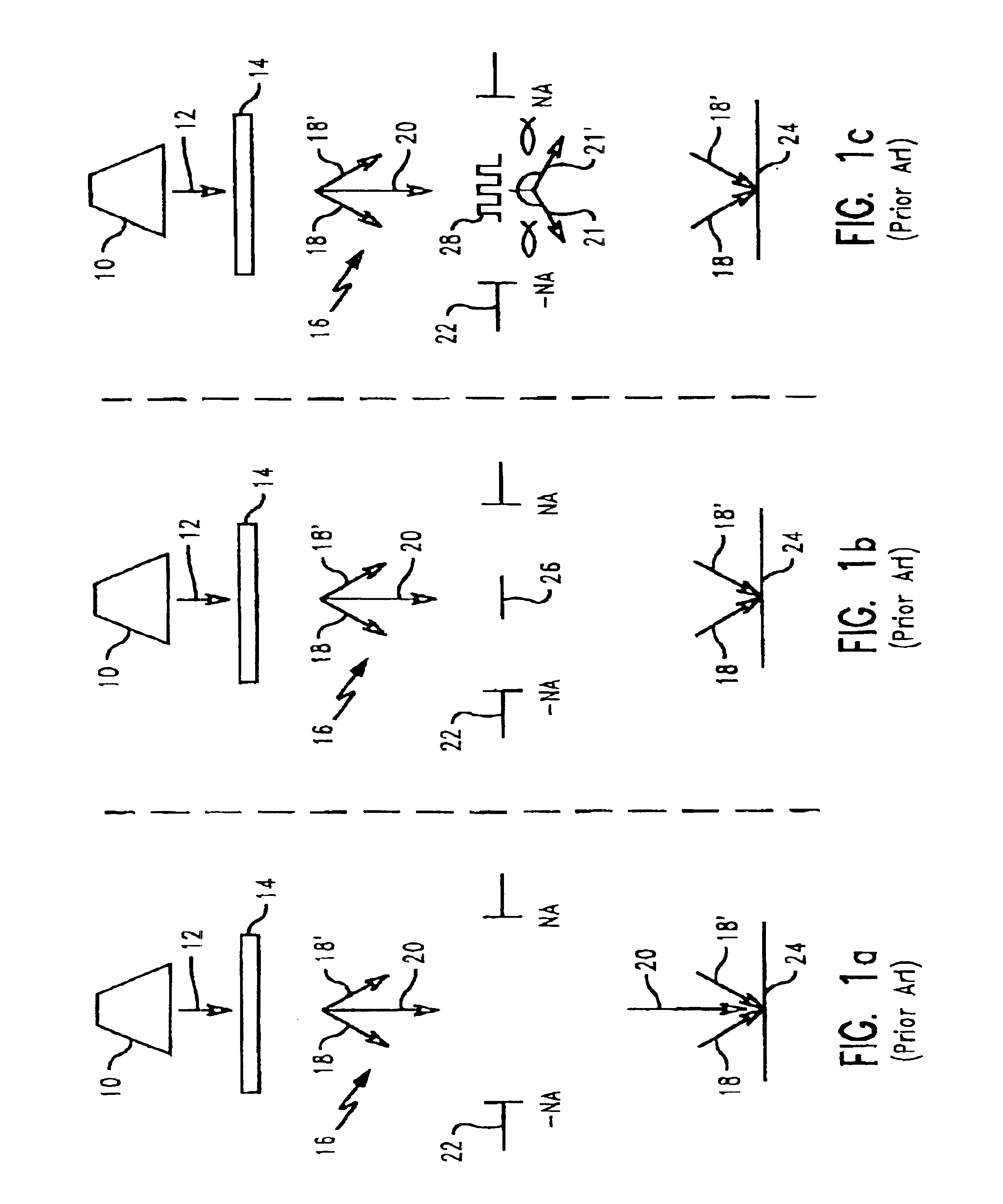
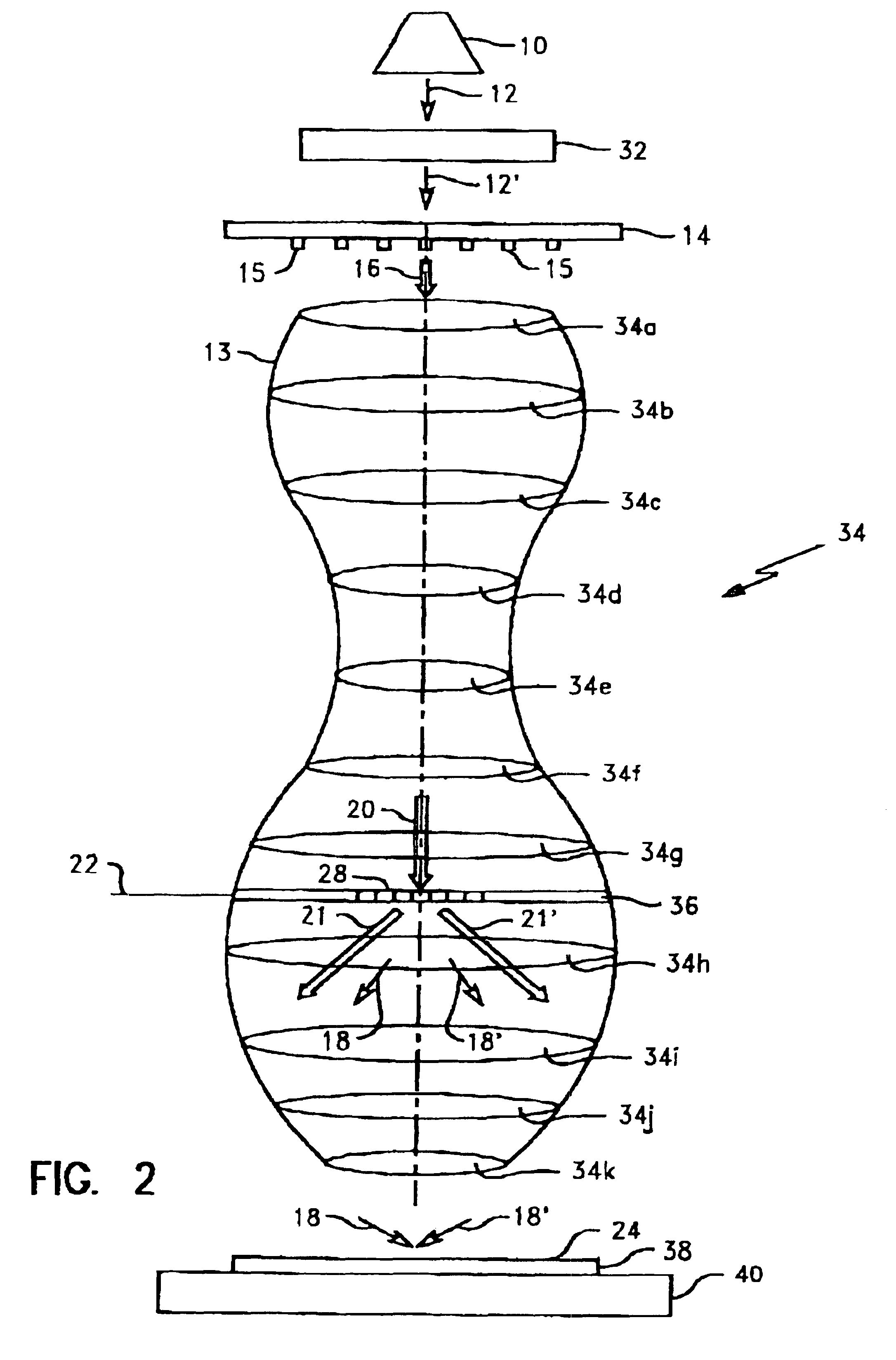
[0019]In describing the preferred embodiment of the present invention, reference will be made herein to FIGS. 1-4 of the drawings in which like numerals refer to like features of the invention.

[0020]A schematic of the preferred projection system, or stepper, of the present invention is depicted in FIG. 2. Illumination source 10 emits light or other energy beam 12, which travels through a condenser lens 32 and onward as beam 12′, through mask 14. Disposed on mask 14 is a mask pattern made up of elements 15 configured to the pattern of the microelectronic circuit elements or other features which are to be lithographically produced on the surface of wafer substrate 38. Wafer substrate 38 is mounted on a workpiece support or stage 40 which moves the wafer as the mask 14 patterns 15 are repeatedly projected onto the image plane of 24 on the surface of the wafer, which contains a resist layer that reacts to the projected pattern. A projection lens system 34 comprises, in sequence, a serie...


PUM

PropertyMeasurementUnit
obtuse angleaaaaaaaaaa
energyaaaaaaaaaa
obtuse angleaaaaaaaaaa

Abstract

A method of projecting a pattern from a mask onto a substrate comprises providing an energy source, a substrate, and a mask containing a pattern of features to be projected onto the substrate, and projecting an energy beam from the energy source though the mask toward the substrate to create a projected mask pattern image. The projected mask pattern image is created by zeroth and higher orders of the energy beam. The method then includes diffracting zeroth order beams of the projected mask pattern image to an extent that prevents the zeroth order beams from reaching the substrate, while permitting higher order beams of the projected mask pattern image to reach the substrate. Preferably, the zeroth order beams of the projected mask pattern image are diffracted at an obtuse angle.

Description

BACKGROUND OF INVENTION[0001]The present invention relates to a method and apparatus for projecting a pattern from a mask onto a substrate in the lithographic production of microelectronic features and, in particular, to a method and apparatus which filters amplitude in the frequency plane of the projected image.[0002]Because of the need to decrease size of microelectronic circuits and other features lithographically produced on semiconductor wafers, there has been considerable effort made to increase the resolution of the image projected onto the substrate from the mask containing the image pattern. Some work has been done to modify the phase of the light beam as it passes through the mask, and other work has been done to modify the amplitude of the energy beam containing the projected mask pattern image. As shown in FIG. 1A in an illustration of a typical prior art projection system, also called a stepper, an illumination source 10 projects an energy beam 12 through a mask 14 cont...

Claims


Application Information

Patent Timeline
Patent Type & Authority Patents(United States)
IPC IPC(8): G03B27/42G03B27/72G02B27/42G03B27/32G02B27/44G03C5/04
CPCG03B27/72G03F7/70316
Inventor BUTT, SHAHIDBURKHARDT, MARTIN
Owner QIMONDA
Why Eureka
Try Eureka