Multichip module package and fabrication method

a technology of multi-chip modules and fabrication methods, applied in the field of semiconductor modules, can solve the problems of increasing the need for higher and higher heat dissipation, the inability to provide customized physical and electrical support, and the limited density of the ic density

Active Publication Date: 2005-09-13
STATS CHIPPAC LTD
View PDF4 Cites 68 Cited by
  • Summary
  • Abstract
  • Description
  • Claims
  • Application Information

AI Technical Summary

Problems solved by technology

However, IC density continues to be limited by several factors.
Another limiting factor is the increasing need for higher and higher heat dissipation due not only to the higher density IC integration levels, but also due to the ever-increasing operating frequencies of the semiconductor devices.
Still another limiting factor is the need to provide customized physical and electrical support for the differing individual needs of the semiconductor devices in such high density configurations.
Unfortunately, existing multichip modules do not satisfactorily meet these requirements.
For example, existing MCM-EBGA designs employ a single heat sink plane and therefore do not make different die backside electrical potentials available for the various semiconductor devices therein.
Thermally enhanced PBGA designs utilize a drop-in heat spreader that accommodates high-power devices that need considerable heat dissipation but cannot support certain different die backside potentials.
Solutions to these problems have been long sought but prior developments have not taught or suggested any solutions and, thus, solutions to these problems have long eluded those skilled in the art.

Method used


Image

  • Multichip module package and fabrication method
  • Multichip module package and fabrication method
  • Multichip module package and fabrication method

Examples


Embodiment Construction

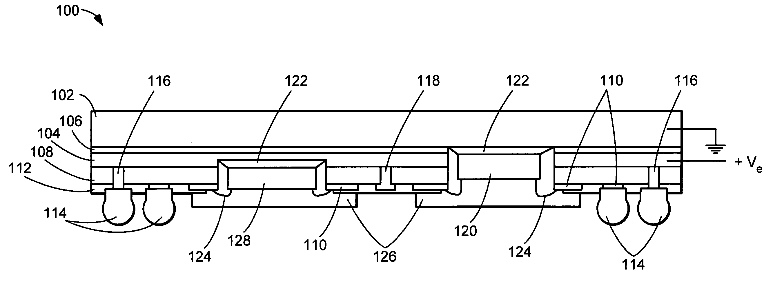
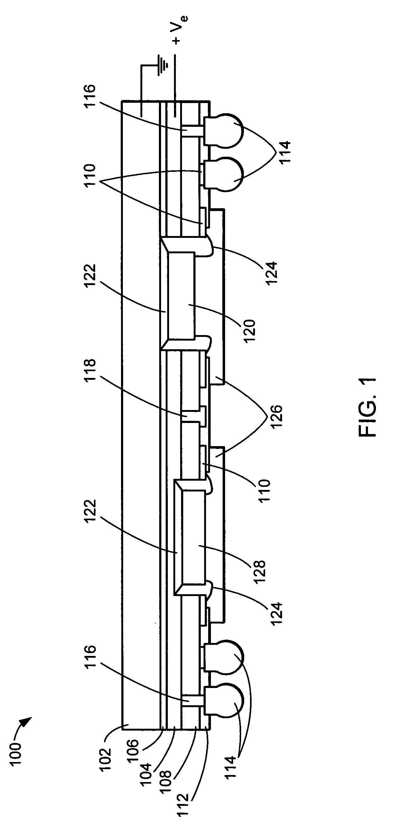
[0018]In the following description, numerous specific details are given to provide a thorough understanding of the invention. However, it will be apparent that the invention may be practiced without these specific details. In order to avoid obscuring the present invention, some well-known package circuit configurations and fabrication process steps are not disclosed in detail. Likewise, the drawings showing embodiments of the device are semi-diagrammatic and not to scale and, particularly, some of the dimensions are for the clarity of presentation and may be exaggerated. Also, for clarity and ease of illustration, description, and comprehension, similar and like features one to another will typically be described with like reference numerals.

[0019]The term “horizontal” as used herein is defined as a plane parallel to the conventional plane or surface of a multichip-module (“MCM”) package, regardless of its orientation. The term “vertical” refers to a direction perpendicular to the h...


PUM


Abstract

A method for fabricating a multichip module package includes providing a first heat sink positioned for releasing heat from the package and providing a second heat sink positioned proximate the first heat sink. The heat sinks are thermally coupled and electrically isolated to and from one another. A first semiconductor device is attached to the first heat sink in thermal and electrical communication therewith and electrically insulated from the second heat sink. A second semiconductor device is attached to the second heat sink in thermal and electrical communication therewith and electrically insulated from the first heat sink.

Description

TECHNICAL FIELD[0001]The present invention relates generally to semiconductor packages, and more particularly to multichip module packages and methods for the fabrication thereof.BACKGROUND ART[0002]The computer industry continually strives toward higher performance, lower cost, increased miniaturization of components, and greater packaging density of integrated circuits (“IC's”). As new generations of IC products are released, their functionality increases while the number of components needed to produce them decreases.[0003]Semiconductor devices are constructed from a silicon (“Si”) or gallium arsenide (“GaAs”) wafer through a process that comprises a number of deposition, masking, diffusion, etching, and implanting steps. Usually, many individual devices are constructed on the same wafer. When the devices are separated into individual rectangular units, each takes the form of an IC die.[0004]In order to interface a die with other circuitry, it is common to mount it on a leadframe...

Claims


Application Information

Patent Timeline
Patent Type & Authority Patents(United States)
IPC IPC(8): H01L21/02H01L21/44
CPCH01L21/50H01L23/13H01L23/36H01L23/49816H01L25/0655H01L24/48H01L2224/48227H01L2924/15321H01L2224/45124H01L2924/00H01L2224/45144H01L2924/00014H01L24/45H01L2924/14H01L2924/181H01L2224/73265H01L2924/00015H01L2224/05599H01L2924/00012
Inventor SHIM, IL KWONFILOTEO, JR., DARIO S.HO, TSZ YINSOON, SEBASTIAN T. M.
Owner STATS CHIPPAC LTD
Why Eureka
Try Eureka