Nonvolatile semiconductor memory device having a two-layer gate structure and method for manufacturing the same

Inactive Publication Date: 2005-09-13
KK TOSHIBA
View PDF14 Cites 21 Cited by
  • Summary
  • Abstract
  • Description
  • Claims
  • Application Information

AI Technical Summary

Benefits of technology

[0012]The present invention solves the above-mentioned task and the object of the present invention is to provide a nonvolatile semi

Problems solved by technology

In the case where, on the other hand, the selection ratio is set smaller, etching is not stopped

Method used


Image

  • Nonvolatile semiconductor memory device having a two-layer gate structure and method for manufacturing the same
  • Nonvolatile semiconductor memory device having a two-layer gate structure and method for manufacturing the same
  • Nonvolatile semiconductor memory device having a two-layer gate structure and method for manufacturing the same

Examples


Example

[0030]The embodiment of the present invention will be explained below with reference to the accompanying drawing.

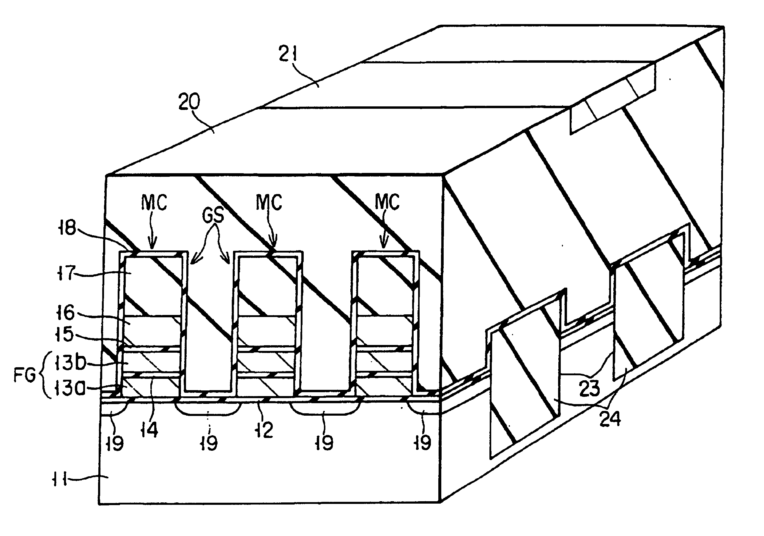
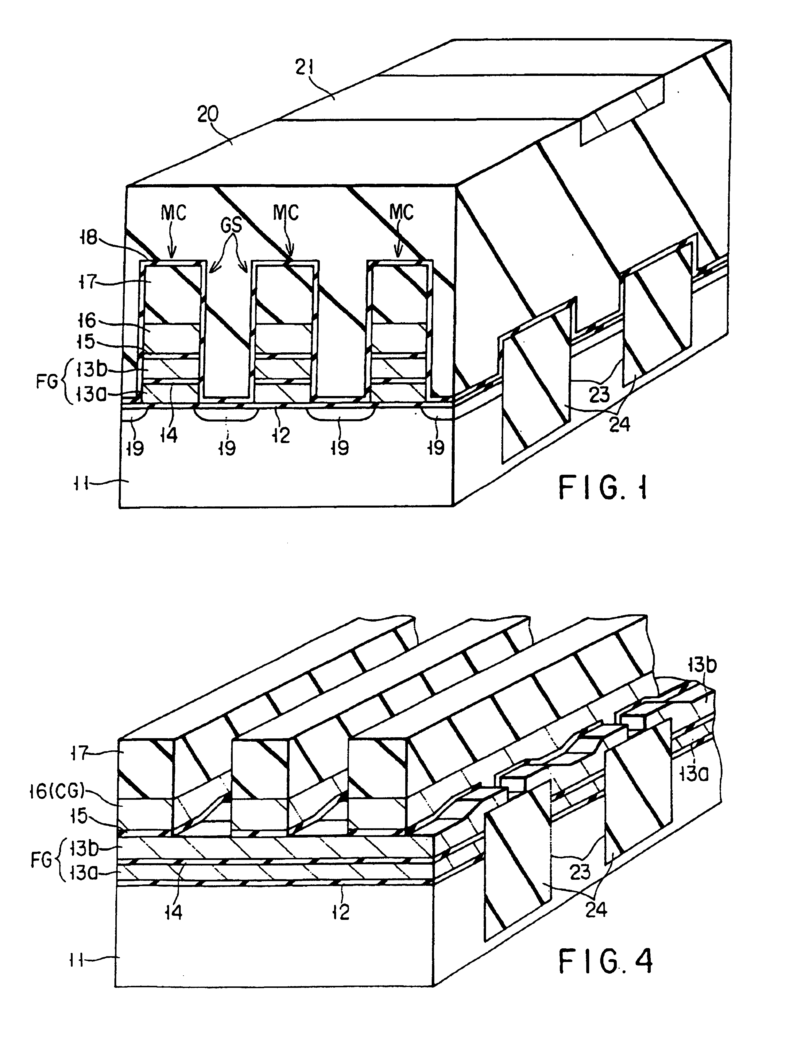
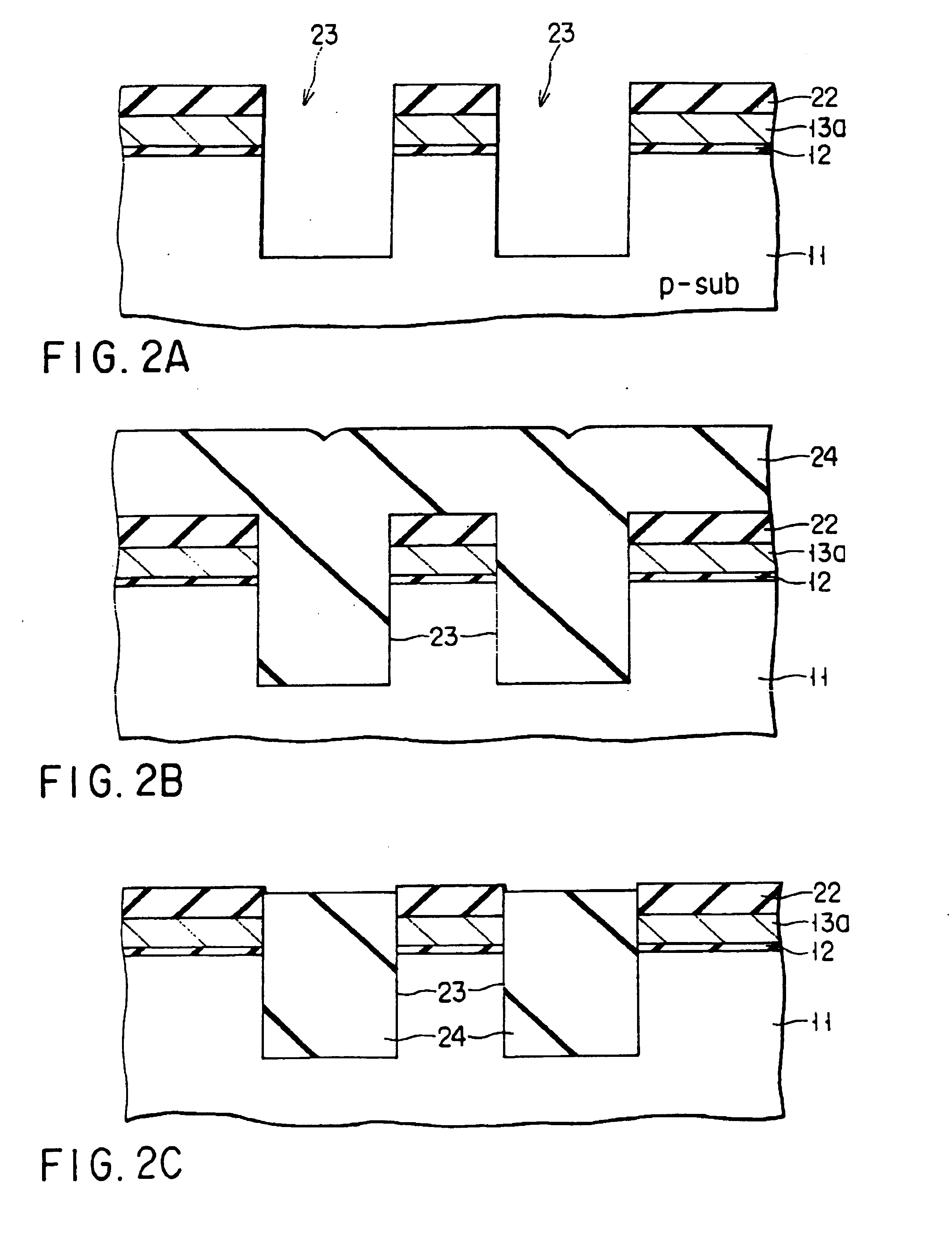
[0031]FIG. 1 shows a nonvolatile semiconductor memory device of the present invention and shows the case where the present invention is applied to a NAND type flash EEPROM for initially forming a gate. In FIG. 1, one NAND cell comprises a plurality of memory cells MC connected in a series array. Each NAND cell is separated by an STI area comprised of a buried insulating film 24 formed in a semiconductor substrate 11 of, for example, a P type.

[0032]In the respective memory cell MC, a gate oxide film 12 is formed on a surface of the semiconductor substrate 11. A first floating gate 13a of, for example, polysilicon is formed on the gate oxide film 12 to provide a floating gate FG. An insulating film 14 constituting the feature of the present invention is formed on a first floating gate 13a. This insulating film 14 is comprised of, for example, a silicon oxide film. A second ...


PUM


Abstract

In a memory cell, a gate oxide film is formed on a surface of semiconductor substrate and a first floating gate is formed on the gate oxide film. An insulating film is formed on a first floating gate and a second floating gate is formed on the insulating film. The first and second floating gates constitute a floating gate in the memory cell. An insulating film between the first floating gate and the second floating gate acts as an etching stopper when a polysilicon constituting the second floating gate is etched.

Description

[0001]This is a Divisional Application of application Ser. No. 09 / 558,585, filed on Apr. 26, 2000 now abandoned. This application is based upon and claims the benefit of priority from the prior Japanese Patent Application No. 11-119848, filed on Apr. 27, 1999, the entire contents of which are incorporated herein by reference.CROSS-REFERENCE TO RELATED APPLICATIONS[0002]This application is based upon and claims the benefit of priority from the prior Japanese Patent Application No. 11-119848, filed Apr. 27, 1999, the entire contents of which are incorporated herein by reference.BACKGROUND OF THE INVENTION[0003]The present invention relates to a nonvolatile semiconductor memory device of a two-layered gate structure, such as a flash EEPROM and a method for manufacturing the same.[0004]In recent years, a NAND cell type EEPROM has been proposed as one of electrically erasable semiconductor memory devices. This NAND cell type EEPROM is of such a type that a plurality of memory cells are p...

Claims


Application Information

Patent Timeline
IPC IPC(8): H01L21/70H01L27/115H01L29/423H01L21/8247H01L29/40H01L29/788H01L29/792
CPCH01L27/115H01L27/11521H01L29/42324H10B69/00H10B41/30
Inventor KAMIYA, EIJISHIMIZU, KAZUHIRO
Owner KK TOSHIBA
Why Eureka
Try Eureka