Method of forming a magnetoresistive device

a technology of magnetoresistive devices and magnetic devices, which is applied in the direction of magnet bodies, manufacturing tools, instruments, etc., can solve the problems of complex processes, high cost, and limited control of track width and throat heigh

Inactive Publication Date: 2005-09-20
WESTERN DIGITAL TECH INC
View PDF53 Cites 158 Cited by
  • Summary
  • Abstract
  • Description
  • Claims
  • Application Information

AI Technical Summary

Benefits of technology

[0014]The present invention provides a method of forming a head such as a read/write head. The read/write head can be, for example, an MR head. An exemplary embodiment of the method comprises forming a write transducer on a wafer, cutting the wafer to produce a slider bar with a cut surface, and planarizing the cut surface of the slider bar. More specifically, forming the write transducer can include forming a first pole layer and forming a first pole pedestal layer over the first pole layer, where the first pole pedestal layer includes a tapered portion defined by a first end having a nose width less than a desired final nose width, and a second end having a zero throat width greater than the desired final nose width. In this exemplary embodiment, planarizing the cut surface of the slider bar

Problems solved by technology

However, the control of trackwidth and throat height can be limited with typical fabrication processes, such as masking and plating at the wafer level.
These problems are further aggravated with increasing topography over which the trackwidth-defining element is formed.
Greater trackwidth control can be attempted using other processes such as focused ion beam (FIB) milling, however such processes can be expensive.
However, such processes can also be expensive, complex, and result in lower production yields.
It can also be very difficult and expensive to form very small trackwidths using typical processes.
Therefore, forming a pole pedestal h

Method used


Image

  • Method of forming a magnetoresistive device
  • Method of forming a magnetoresistive device
  • Method of forming a magnetoresistive device

Examples


Embodiment Construction

[0029]FIGS. 1A, 1B, and 2A–2C have been described above with reference to the prior art.

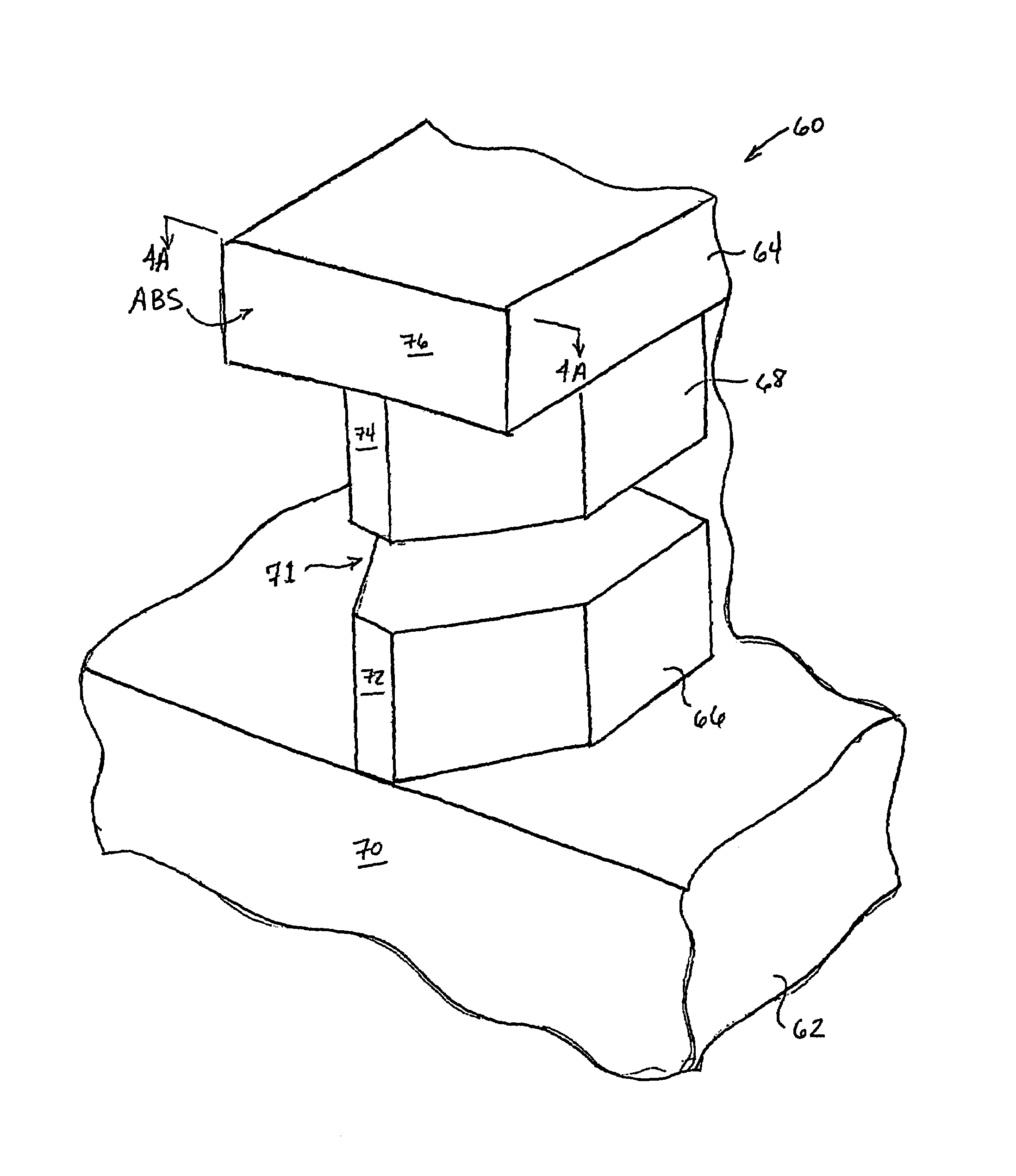
[0030]FIG. 3 is a perspective view of a pole tip portion of a write element 60, according to an embodiment of the present invention. The write element 60 includes a first pole 62 and second pole 64, formed of a magnetic material, similar to those of the prior art. A first pole pedestal 66 is also formed of magnetic material and is magnetically connected to the first pole 62. A second pole pedestal 68 formed of magnetic material is magnetically connected to the second pole 64. Also, the first pole 62 includes a first pole first surface 70 which forms a portion of the air bearing surface ABS. A first pole pedestal first surface 72, and a second pole pedestal first surface 74 are also included in the air bearing surface ABS, along with a second pole first surface 76. The first pole pedestal 66 and second pole pedestal 68 are disposed between the first pole 62 and the second pole 64 and further defin...


PUM

PropertyMeasurementUnit
Widthaaaaaaaaaa
Heightaaaaaaaaaa
Magnetoresistanceaaaaaaaaaa

Abstract

A method of forming a head comprises forming a write transducer on a wafer, cutting the wafer to produce a slider bar with a cut surface, and planarizing the cut surface of the slider bar. Forming the write transducer can include forming a first pole layer and forming a first pole pedestal layer over the first pole layer, where the first pole pedestal layer includes a tapered portion defined by a first end having a nose width less than a desired final nose width, and a second end having a zero throat width greater than the desired final nose width. Planarizing the cut surface of the slider bar exposes the first pole pedestal layer until a width thereof approximately equals the desired final nose width.

Description

CROSS-REFERENCE TO RELATED APPLICATIONS[0001]This application is a divisional of U.S. application Ser. No. 10 / 013,431 filed on Dec. 11, 2001, now U.S. Pat. No. 6,829,819, which is a divisional of U.S. application Ser. No. 09 / 304,224 filed on May 3, 1999, now abandoned, and claims priority therefrom pursuant to 35 U.S.C. § 120.BACKGROUND OF THE INVENTION[0002]1. Field of the Invention[0003]This divisional application relates generally to magnetic disk data storage systems, and more particularly to methods for making magnetic write transducers.[0004]2. Description of the Background Art[0005]Magnetic disk drives are used to store and retrieve data for digital electronic apparatuses such as computers. In FIGS. 1A and 1B, a magnetic disk data storage systems of the prior art includes a sealed enclosure 12, a disk drive motor 14, a magnetic disk 16, supported for rotation by a drive spindle S1 of motor 14, an actuator 18 and an arm 20 attached to an actuator spindle S2 of actuator 18. A s...

Claims


Application Information

Patent Timeline
IPC IPC(8): G11B5/127H04R31/00G11B5/39
CPCG11B5/39Y10T29/49073Y10T29/49048Y10T29/49071Y10T29/49041Y10T29/49043Y10T29/49046Y10T29/49798
Inventor CRUE, JR., BILLY W.THOMAS, MARK DAVIDSHI, ZHUPEIAPPARAO, RENUKA
Owner WESTERN DIGITAL TECH INC
Why Eureka
Try Eureka