Real time analysis of periodic structures on semiconductors

a technology of periodic structure and real-time analysis, applied in the field of data analysis, can solve the problems of large spot size of conventional optical probe beams, scatterometry techniques, and limited technology suitable for measuring these small periodic features (critical dimensions), and achieve the effect of accurately modeling and high density of layers

Inactive Publication Date: 2005-09-20
THERMA WAVE INC
View PDF23 Cites 17 Cited by
  • Summary
  • Abstract
  • Description
  • Claims
  • Application Information

AI Technical Summary

Benefits of technology

[0018]During these iterative steps, the thickness of the layers (density of the layers) are permitted to vary in a manner so that a higher density of layers will be placed in regions where the change in width is the greatest. In this way, the curvature of the side walls can be most accurately modeled.
[0020]The scatterometry calculations associated with the early iterations of the models (square, trapezoid) are relatively simple and fast. However, as the number of widths and layers increase, the calculations become exponentially more difficult.

Problems solved by technology

Technologies suitable for measuring these small periodic features (critical dimensions) are quite limited.
However, the smallest spot size of conventional optical probe beams is larger than the size of the periodic features which need to be measured.
The difficulty in directly measuring such small structures has lead to the development of scatterometry techniques.
The calculations discussed above are relatively complex even for the most simple models.
As the models become more complex (particularly as the profiles of the walls of the features become more complex) the calculations become exceedingly long and complex.
Even with today's high speed processors, the art has not developed a suitable approach for analyzing more complex structures to a highly detailed level on a real time basis.
While the use of libraries does permit a relatively quick analysis to be made after the sample has been measured, it is not entirely satisfactory for a number of reasons.
In addition, the accuracy of the results is limited by the number of models stored in the library.
The more models that are stored, the more accurate the result, however, the longer it will take to create the library and the longer it will take to make the comparison.
However, the authors note that performing an analysis with 40 variables (the width and height of 20 slabs) would be too computationally complex.
While such an approach achieves the goal of reducing computational complexity, it does so at the expense of limiting the accuracy of the analysis.

Method used


Image

  • Real time analysis of periodic structures on semiconductors
  • Real time analysis of periodic structures on semiconductors
  • Real time analysis of periodic structures on semiconductors

Examples


Embodiment Construction

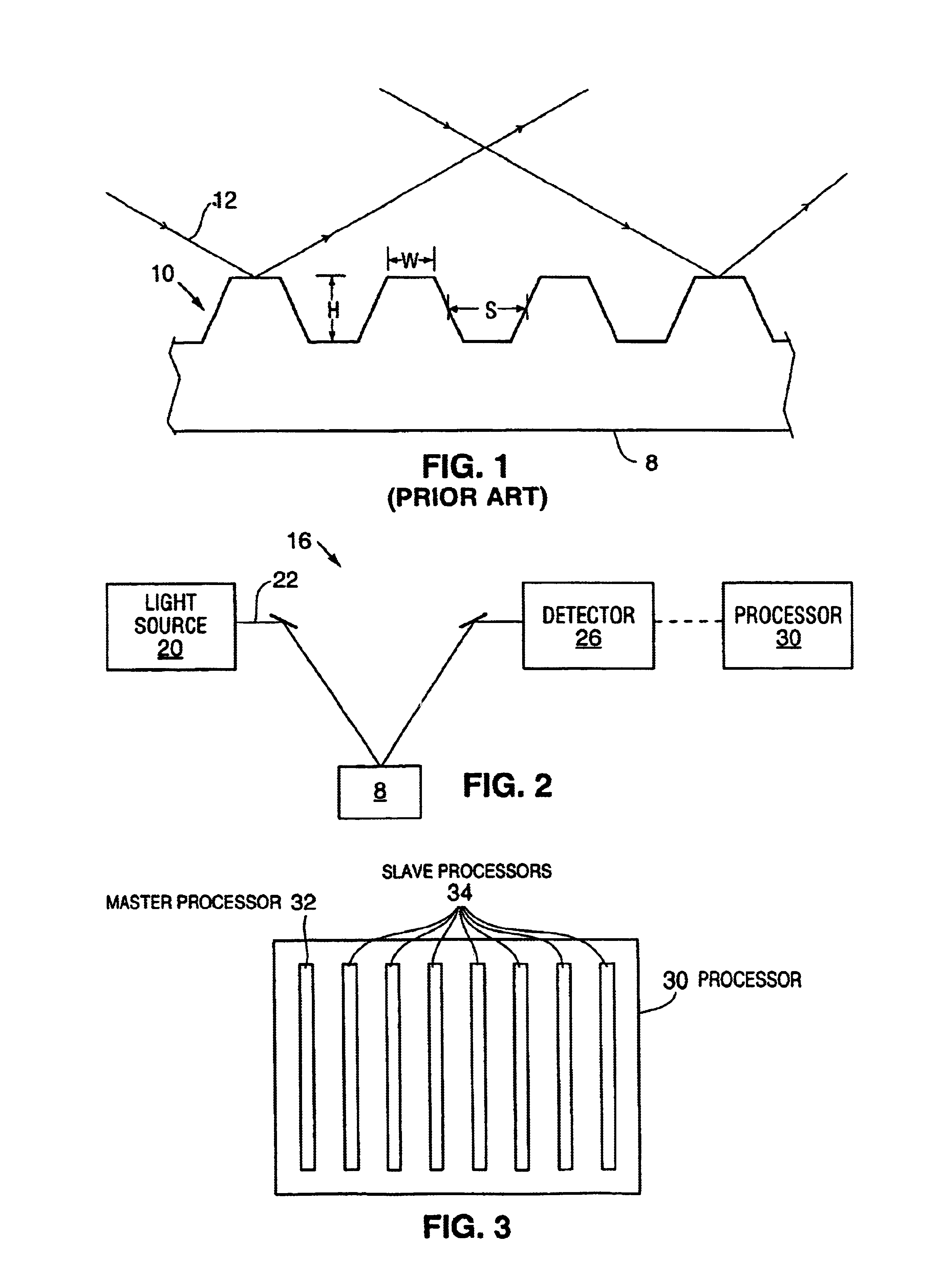
[0033]FIG. 2 is a block diagram of a system 16 for performing scatterometry measurements on a sample 8 having a periodic structure. For the purposes of this disclosure, the periodic structure means any repeating feature, where the feature size is about the same or smaller than the beam of light probing the sample such that at least some of the light is scattered rather than specularly reflected.

[0034]The system 16 includes a light source 20. As noted above, scatterometry measurements are often made using a broad band light source generating a probe beam 22 having a plurality of wavelengths. As described in U.S. Pat. No. 6,429,943, cited above, the light can also be from a laser. In such a case, measurements would be taken as a function of angle of incidence, preferably without moving the sample.

[0035]Probe beam is directed to the sample. Typically a lens (not shown) is used to focus the probe beam to a small spot on the sample. The reflected probe beam is captured and measured by de...


PUM

PropertyMeasurementUnit
spectroscopic ellipsometeraaaaaaaaaa
wavelengthaaaaaaaaaa
wavelengthsaaaaaaaaaa

Abstract

A system for characterizing periodic structures on a real time basis is disclosed. A multi-parameter measurement module generates output signals as a function of wavelength or angle of incidence. The output signals are supplied to a parallel processor, which creates an initial theoretical model and calculates the theoretical optical response. The calculated optical response is compared to measured values. Based on the comparison, the model configuration is modified to be closer to the actual measured structure. Thereafter, the complexity of the model is iteratively increased, by dividing the model into layers each having an associated width and height. The model is fit to the data in an iterative manner until a best fit model is obtained which is similar in structure to the periodic structure.

Description

PRIORITY[0001]This application is a continuation of U.S. application Ser. No. 09 / 906,290, filed Jul. 16, 2001, now issued U.S. Pat. No. 6,704,661.TECHNICAL FIELD[0002]The subject invention relates to the analysis of data obtained during the measurement of periodic structures on semiconductors. In particular, an approach is disclosed which allows accurate, real time analysis of such structures.BACKGROUND OF THE INVENTION[0003]The semiconductor industry is continually reducing the size of features on wafers. These features include raised profiles and trenches that have a particular height (or depth), width and shape (contour). Accurate measurement of these features is necessary to insure appropriate yields.[0004]Technologies suitable for measuring these small periodic features (critical dimensions) are quite limited. Optical measurement technology is the most desirable since it is a non-contact technique. However, the smallest spot size of conventional optical probe beams is larger th...

Claims


Application Information

Patent Timeline
Patent Type & Authority Patents(United States)
IPC IPC(8): G03F7/20G01B11/02G01B11/24G01N21/21G01N21/27G06F17/00H01L21/027H01L21/66
CPCG01B11/24G01N21/211G03F7/705G03F7/70616G03F7/70625
Inventor OPSAL, JONCHU, HANYOU
Owner THERMA WAVE INC
Why Eureka
Try Eureka