Unlock instant, AI-driven research and patent intelligence for your innovation.

Defect inspection apparatus

a technology of inspection apparatus and defect, applied in the field of inspection apparatus, can solve problems such as difficulty in taking measures and irregular line width

Inactive Publication Date: 2005-10-11
OLYMPUS CORP
View PDF15 Cites 10 Cited by
  • Summary
  • Abstract
  • Description
  • Claims
  • Application Information

AI Technical Summary

Benefits of technology

[0013]The present invention provides a defect inspection apparatus comprising: an inspection section which inspects a front surface and a rear surface of a sample; a control section which processes image data on the front surface and rear surface of the sample obtained by the inspection section; moving section provided in the inspection section and capable of reciprocating the sample; illumination secti

Problems solved by technology

However, in the photolithography process, if the resist applied to a substrate surface has an uneven film or dust sticking thereto, the uneven film or dust causes such defects as an irregular line width of the pattern or pin holes in the pattern after etching.
However, under a current situation, even when the peripheral portions of the rear surface of the sample 1 bulge, or the rear surface of the sample 1 has flaws or dust sticking thereto, it is difficult to take measures for these problems because a technique described in the above-mentioned publication does not provide means to detect the rear surface of the sample.

Method used


Image

  • Defect inspection apparatus
  • Defect inspection apparatus
  • Defect inspection apparatus

Examples


first embodiment

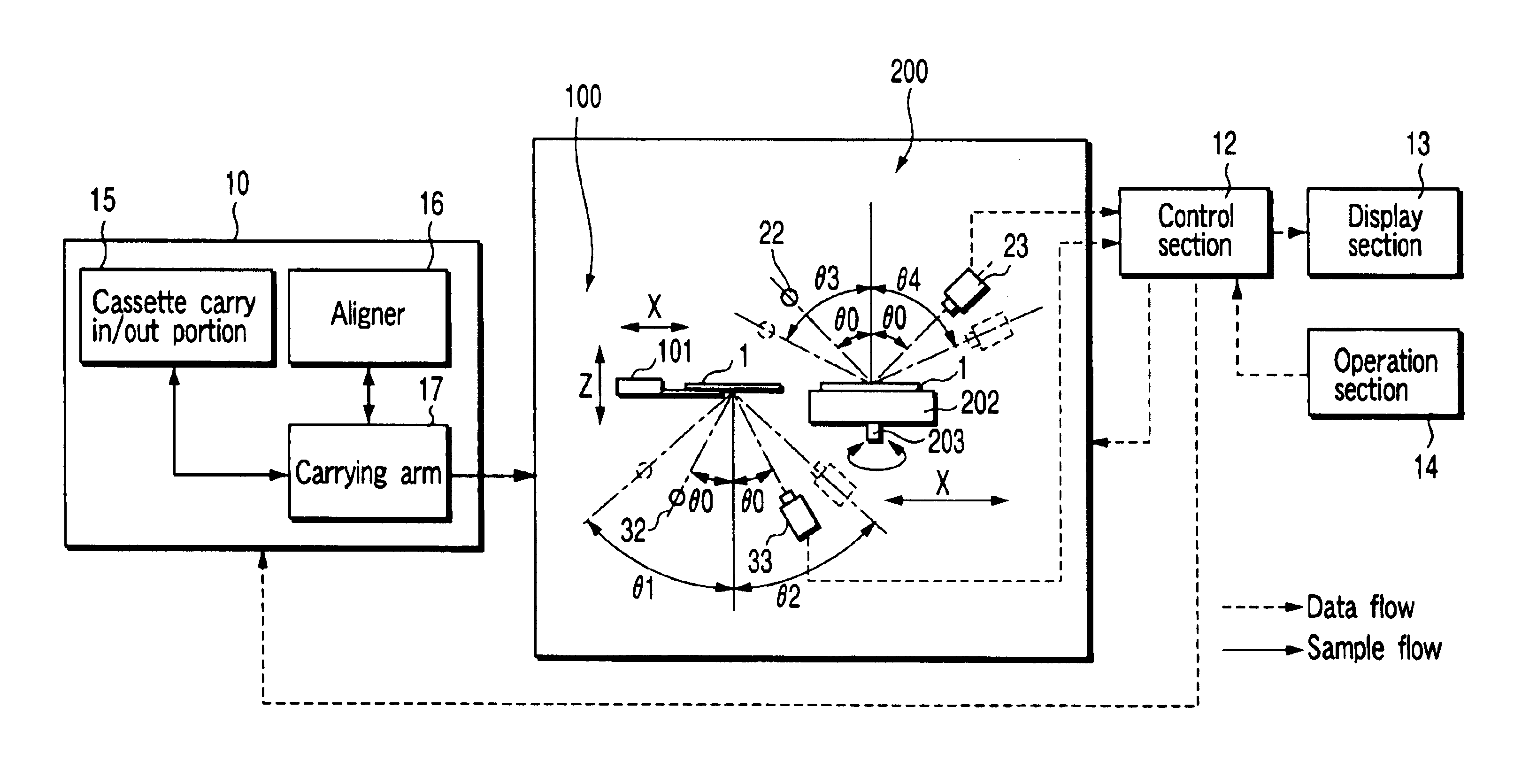
[0030]FIG. 1 is a diagram showing a configuration of a defect inspection apparatus according to the present invention. In FIG. 1, arrows with broken lines indicate flow of data, and arrows with full lines indicate flow of a sample 1.

[0031]This defect inspection apparatus performs a defect inspection of the sample 1 including, for example, a semiconductor wafer or a glass substrate of a flat display. This defect inspection apparatus is generally comprised of a carrying section 10, an inspection section 11 performing the defect inspection of front and rear surfaces of the sample 1, a control section 12 which controls overall operation of the defect inspection, a display section 13 including, for example, a liquid crystal display with a touch sensor for displaying defect inspection results and the like, and an operation section 14 including, for example, a key board and a track ball for operating and inputting instructions and the like for the operation of the defect inspection.

[0032]T...

second embodiment

[0069]FIG. 4 is a diagram showing the configuration of the defect inspection apparatus according to the present invention. In FIG. 4, like numerals are given to like parts of FIG. 1 and are not described.

[0070]An inspection section 30 is provided with a holding member 31 formed of a light-transmitting material such as a glass material or transparent ceramic material. This holding member 31 comprises means for holding the entire surface or peripheral portion of the sample 1. The holding member 31 is capable of reciprocating movement in an X axis direction while holding the sample 1 as above. Above the holding member 31 (the front surface side of the sample 1), the linear light source 22 and the line sensor camera 23 are provided. Under the holding member 31 (the rear surface side of the sample 1), a linear light source 32 and a line sensor camera 33 are provided.

[0071]The linear light source 32 is set at the light irradiation angle θ0 to obtain a regular reflection image on the rear ...

third embodiment

[0088]FIG. 5 is a diagram showing the configuration of the defect inspection apparatus according to the present invention. In FIG. 5, like numerals are given to like parts of FIG. 1 and FIG. 4.

[0089]An inspection section 40 is provided with a holding member 41 which stands the sample 1 and holds the edge of the sample 1. This holding member 41 has the same shape and function as, for example, that of the holding member 24 shown in FIG. 3A and FIG. 3B described above. The holding member 41 is capable of, while standing the sample 1, reciprocating movement in a Z axis direction (upward and downward).

[0090]Therefore, the linear light source 22 and the line sensor camera 23 are provided on one surface side of the standing holding member 41 (the front surface side of the sample 1). The linear light source 32 and the line sensor camera 33 are provided on the other surface side of the holding member 41 (the rear surface side of the sample 1). The present third embodiment is different from t...


PUM


Abstract

The present invention provides a defect inspection apparatus comprising an inspection section which inspects a front surface and a rear surface of a sample, a control section which processes image data on the front surface and rear surface of the sample obtained by the inspection section, moving section provided in the inspection section and capable of reciprocating the sample, illumination section which illuminates the front surface and rear surface of the sample moved by the moving section, and image pickup section which picks up images of the front surface and rear surface of the sample illuminated by the illumination section, wherein at least one of an incidence angle of the illumination section on the sample and an image pickup angle of the image pickup section to the sample is changeable.

Description

CROSS-REFERENCE TO RELATED APPLICATIONS[0001]This is a Continuation Application of PCT Application No. PCT / JP02 / 09762, filed Sep. 24, 2002, which was not published under PCT Article 21(2) in English.[0002]This application is based upon and claims the benefit of priority from prior Japanese Patent Applications No. 2001-289963, filed Sep. 21, 2001; and No. 2002-080836, filed Mar. 22, 2002, the entire contents of both of which are incorporated herein by reference.BACKGROUND OF THE INVENTION[0003]1. Field of the Invention[0004]The present invention relates to a defect inspection apparatus which applies illumination light to a sample such as a semiconductor wafer or a glass substrate of a flat display (FPD), and picks up an image of the light from the sample at this moment to perform defect inspection of the sample from image data thereof.[0005]2. Description of the Related Art[0006]Generally, in the middle of a manufacturing process of, for example, a semiconductor wafer or a glass subs...

Claims


Application Information

Patent Timeline
IPC IPC(8): G01N21/88G01N21/95
CPCG01N21/88G01N21/8806G01N21/9501G01N2021/8841
Inventor NAIKI, HIROSHITANAKA, TOSHIHIKO
Owner OLYMPUS CORP