

Flip-chip BGA semiconductor device for achieving a superior cleaning effect
- Summary
- Abstract
- Description
- Claims
- Application Information
AI Technical Summary
Benefits of technology
Problems solved by technology
Method used
Image

Examples
first embodiment
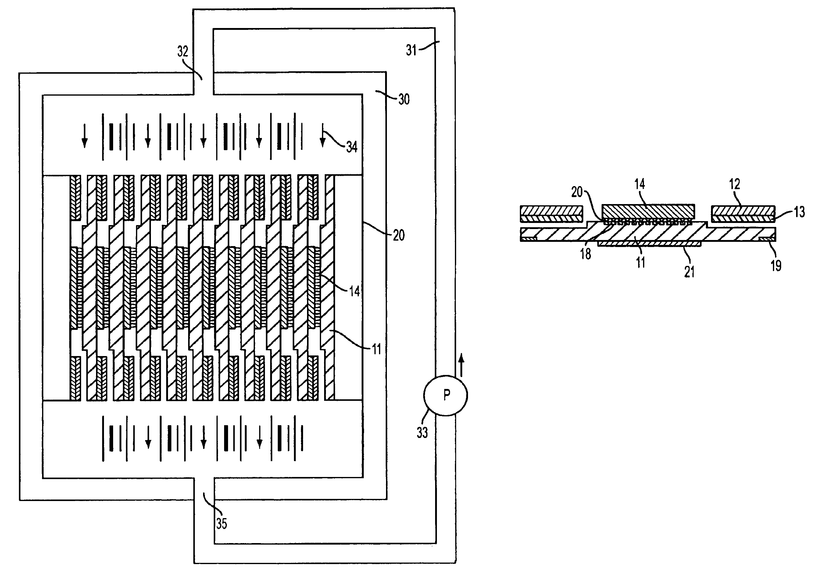
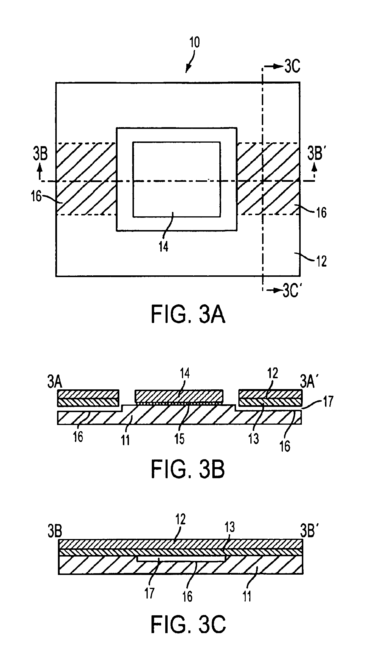
[0032]We first refer to FIGS. 3a to 3c, FIG. 4 and FIG. 6 in accompaniment with the flow chart of FIG. 5 to explain the assembly steps of the flip-chip BGA of the present invention.
[0033]To fabricate flip-chip BGA 10, substrate 11 to which stiffener 12 is attached by adhesive 13 is first prepared, as shown in FIGS. 3a to 3c. An epoxy resin or a mixture of an epoxy resin and olefin resin can be used as adhesive 13.
[0034]An opening is formed in stiffener 12 in the vicinity of the center of substrate 11, and electrodes 18 for connecting the semiconductor chip are arranged in the portion of the surface of substrate 11 that is exposed by this opening, as shown in FIG. 6. In addition, electrodes 19 for connecting to the outside are arranged on the surface of the side of substrate 11 that is opposite the surface on which stiffener 12 is attached; and electrodes 18 for connecting to a semiconductor chip and electrodes 19 for connecting to the outside are connected by way of wired circuits (...
second embodiment
[0042]We next refer to FIGS. 7a to 7c to describe the flip-chip BGA according to the present invention.
[0043]In contrast to flip-chip BGA 10 of the first embodiment in which depressions 16 were provided in substrate 11 to form gaps 17, in the present embodiment, depressions 46 are provided in stiffener 42 to form gaps 47.
[0044]As in the first embodiment, as gaps 47, passages that communicate with the opening of stiffener 42 for mounting semiconductor chip 44 are provided on two opposing sides with the opening interposed.
[0045]Flip-chip BGAs 40 of this embodiment can also be cleaned in cleaning tank 30 that is shown in FIG. 2. In this case, flip-chip BGAs 40 of this embodiment are configured such that jet current 34 that passes through gap 47 between stiffener 42 and substrate 41 (adhesive 43) advances directly to strike against semiconductor chip 44, whereby jet current 34 can be directed substantially directly toward the spaces between balls 45, whereby an excellent cleaning effect...
PUM
 Abstract
Description
Claims
Application Information