In-situ wear indicator for non-selective material removal systems

a non-selective material removal and wear indicator technology, applied in the field of semiconductor process monitoring, can solve the problems of increased number of damaged products, rapid wear to the involved tooling, and degradation of the components of the tooling of the system

Inactive Publication Date: 2005-10-25
INT BUSINESS MASCH CORP
View PDF5 Cites 22 Cited by
  • Summary
  • Abstract
  • Description
  • Claims
  • Application Information

AI Technical Summary

Benefits of technology

[0009]It is an object of the present invention to provide an in-situ indicator for semiconductor manufacturing systems having harsh environments where the indicator is simple, real-time, point of use and can be used in new systems or retrofitted to existing systems.
[0010]It is another object of the invention to provide a method of simply and in real-time determining the ideal or optimum replacement interval for the various elements of a semiconductor manufacturing system.

Problems solved by technology

The manufacture of semiconductors often includes steps that occur in an environment which causes rapid wear to the involved tooling.
Wear to the latches and springs causes inefficient latching that leads to an increased number of damaged products.
However, the non-selective nature of the system results in degradation to elements of the tooling of the system such as the latches on the tool stage, springs or shields.
Eventually, the degradation reaches a point where the elements of the tool system need to be replaced.
It has heretofore been difficult to determine the ideal or optimum replacement interval for the various elements of the system.

Method used


Image

  • In-situ wear indicator for non-selective material removal systems
  • In-situ wear indicator for non-selective material removal systems
  • In-situ wear indicator for non-selective material removal systems

Examples


Embodiment Construction

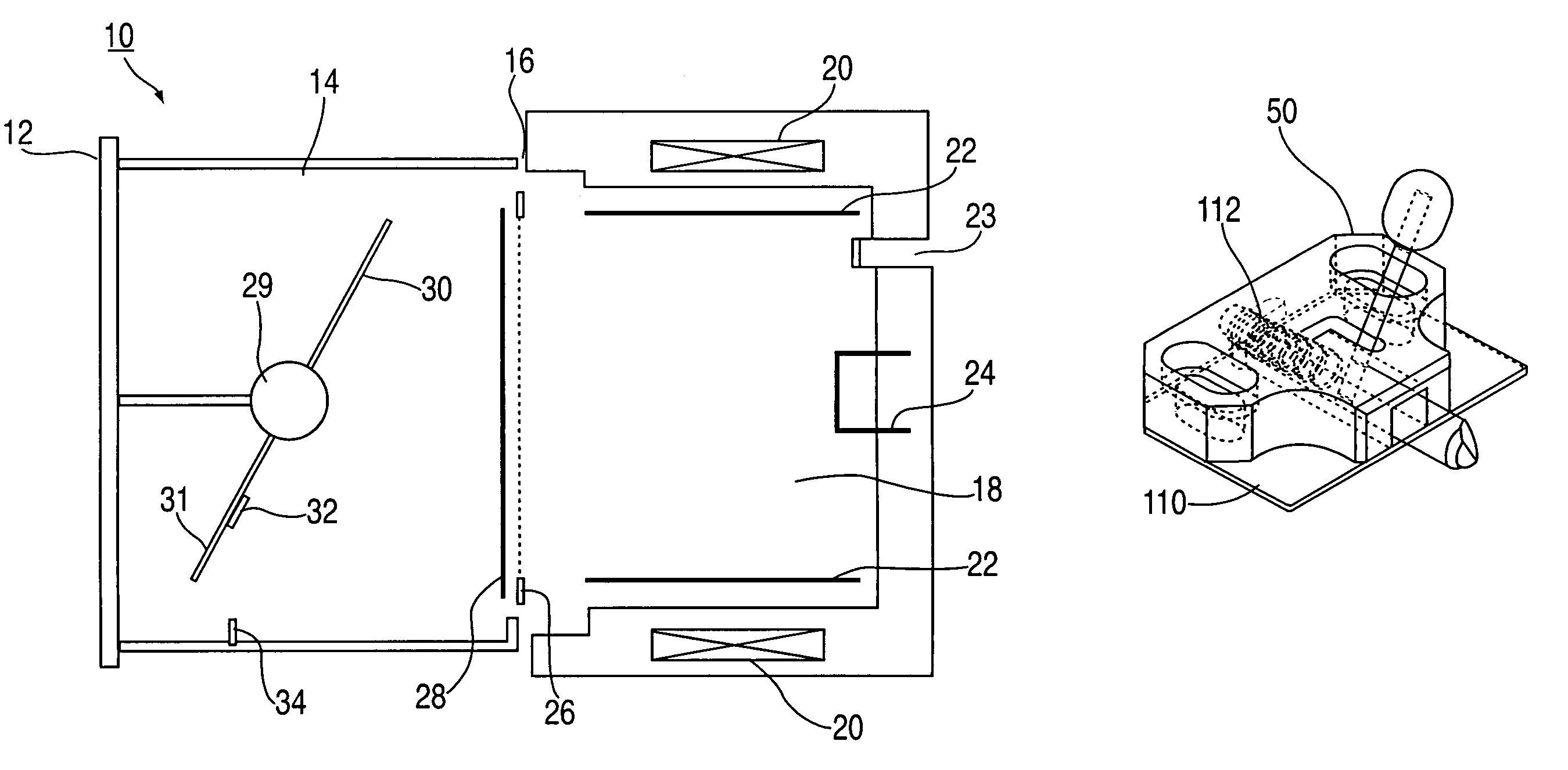
[0017]Although we herein describe the invention as it is used in an ion beam etch system, one skilled in the art would recognize that the invention can be used in any semiconductor manufacturing environment / process that by its nature degrades the parts of the tooling stage, including but not limited to both deposition and removal systems. The typical ion beam etch system and its many components are well known to those skilled in the art. By example, commercial ion beach etch systems are available from Veeco Instruments, Inc.

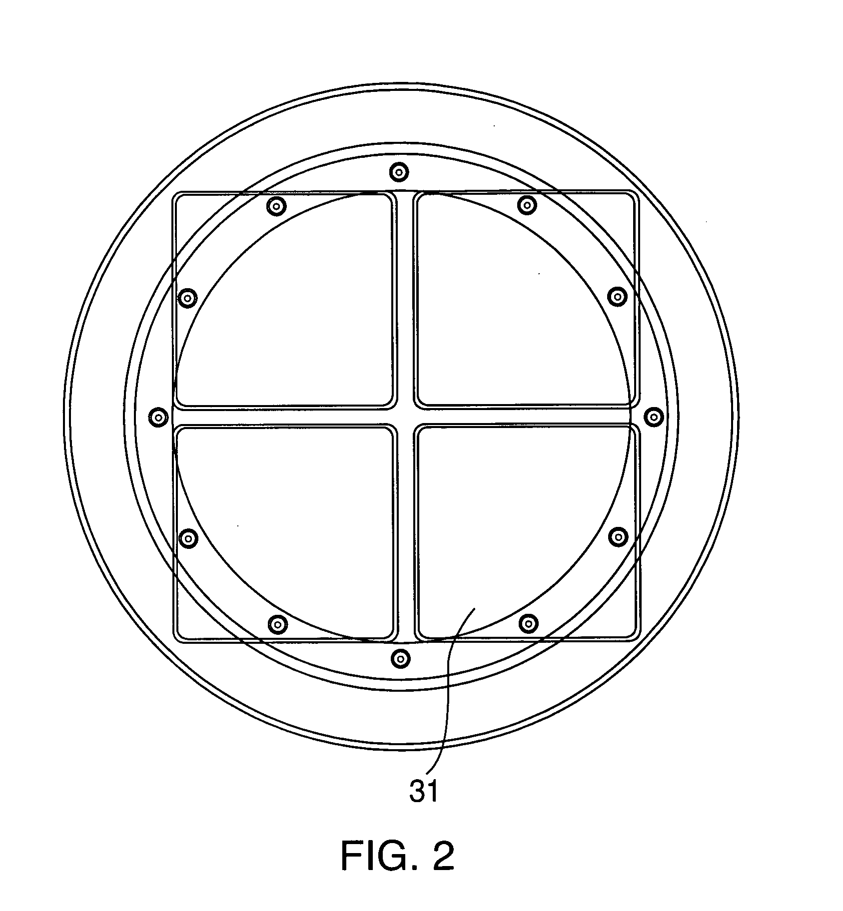
[0018]Referring now to FIG. 1, the present invention is embodied in a system 10 that includes a work chamber 14. The work chamber 14 is accessed through a chamber door 12. The work chamber 14 is connected to a discharge chamber 18 and is separated by a source flange 16. The work chamber includes a rotating fixture 29 upon which is mounted an etch stage 30. The etch stage 30 includes hold down plates 31 that are used to mount the product or substrate, which in mos...


PUM

PropertyMeasurementUnit
energyaaaaaaaaaa
shapeaaaaaaaaaa
thicknessaaaaaaaaaa

Abstract

An in-situ wear indicator for detecting wear to at least one selected part in a semiconductor manufacturing environment. The indicator is manufactured in a selected material with a selected thickness so that the indicator degrades upon exposure to the semiconductor manufacturing process at a fixed rate relative to the wear of the selected part. The indicator displays a visual indication of wear which is discernible by an automated detection device.

Description

BACKGROUND OF THE INVENTION[0001]The invention relates to semiconductor process monitoring, and more specifically relates to an apparatus and method for determining wear indication in semiconductor manufacturing processes such ion beam etching systems and ion beam deposition systems.[0002]The manufacture of semiconductors often includes steps that occur in an environment which causes rapid wear to the involved tooling. Examples of such systems include both deposition / implantation systems and material removal systems. The preferred embodiment of the invention that is disclosed herein is directed to a non-selective material removal system, but one skilled in the art would easily recognize that the invention could be utilized in any semiconductor manufacturing system that causes wear to the tooling in the system due to the harsh environment in certain steps of the semiconductor manufacturing system.[0003]The tooling in the semiconductor environment includes latches and springs that are...

Claims


Application Information

Patent Timeline
Patent Type & Authority Patents(United States)
IPC IPC(8): G01D11/00G01D21/00G01N3/56G01N33/00
CPCG01N3/56G01N2033/0095
Inventor BOETTCHER, GREGORY S.GOLD, STEVEN B.KATZ, ROBERT P.MOORE, GABRIEL V.
Owner INT BUSINESS MASCH CORP
Why Eureka
Try Eureka