High throughput chemical mechanical polishing composition for metal film planarization

a technology of chemical mechanical polishing and composition, applied in metal-working equipment, electrical equipment, lapping machines, etc., can solve the problems of oxide erosion, loss of wafer surface planarity and uniformity,

Inactive Publication Date: 2008-10-16
ADVANCED TECH MATERIALS INC
View PDF31 Cites 82 Cited by
  • Summary
  • Abstract
  • Description
  • Claims
  • Application Information

AI Technical Summary

Benefits of technology

[0022]Other aspects, features and embodiments of the invention will be more fully apparent from the ensuing disclosure and appended claims.

Problems solved by technology

Unfortunately, the “soft landing” and the over-polishing steps often result in dishing and / or erosion into copper features and thus, loss of wafer surface planarity and uniformity.
Dishing occurs when the copper and barrier material removal rates are disparate and as such, too much copper is removed such that the copper surface in the feature is recessed relative to the barrier and / or dielectric surface of the microelectronic device wafer.
Oxide erosion occurs when too much dielectric material is removed.

Method used


Image

  • High throughput chemical mechanical polishing composition for metal film planarization
  • High throughput chemical mechanical polishing composition for metal film planarization
  • High throughput chemical mechanical polishing composition for metal film planarization

Examples


example 1

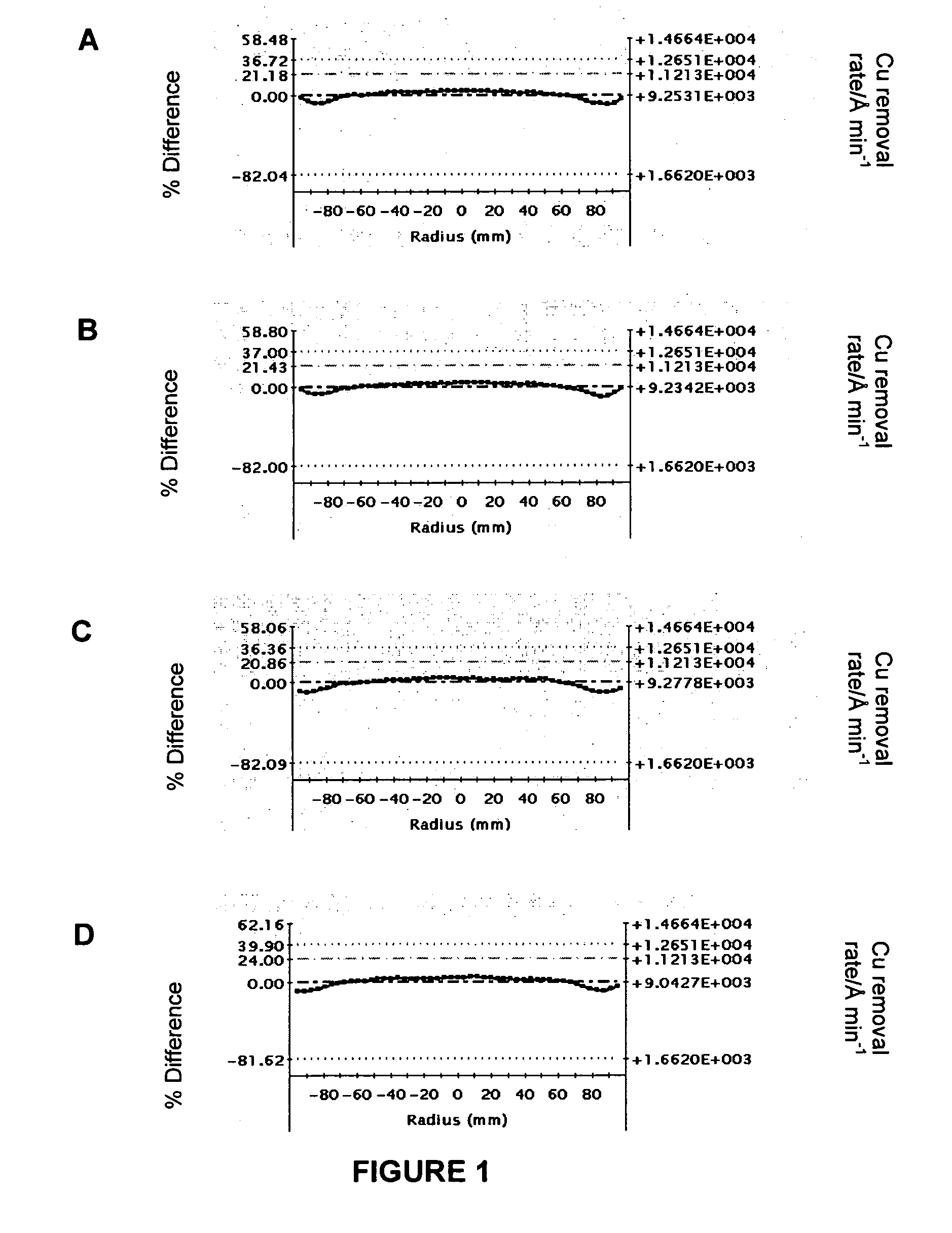
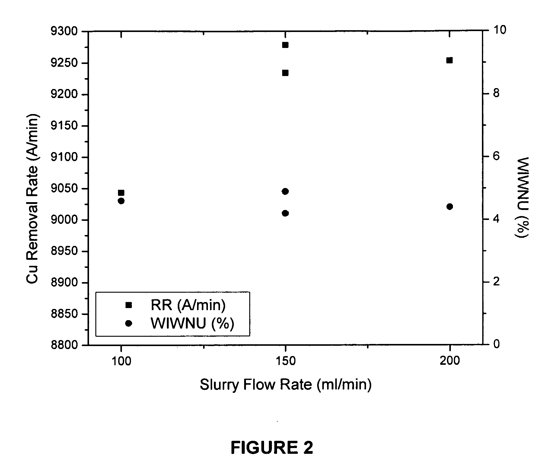
[0098]An experiment was performed to determine the optimum delivery flow rate of bulk copper removal formulation to platen 1 during bulk copper removal. Blanket wafers, having a silicon substrate, a dielectric layer, barrier layer, and a 15,000 Å copper layer, were processed using the bulk copper removal formulation on platen 1 of a Mirra tool. The downforce of the platen 1 was 3 psi. The results, including Cu removal rate and within wafer non-uniformity (WIWNU), are illustrated in FIG. 1 and summarized in Table 1 below.

TABLE 1Bulk copper removal formulation flow rateversus copper removal rate and WIWNU.Bulk Cu removalformulation flow rateCu removal rate (RR)(mL min−1)(Å min−1)WIWNU %Figure20092534.381%1A15092344.202%1B15092784.888%1C10090434.643%1D

[0099]Referring to FIG. 2, it can be seen that the flow rate of the bulk copper removal formulation to platen 1 can be reduced from 200 mL min−1 to 150 mL min−1 without any significant loss in copper removal rate or changes to the WIWNU %...

example 2

[0100]An experiment was performed to demonstrate the utility of the present invention. As discussed previously, it is an object of the present invention to provide a process including a single bulk copper removal CMP slurry formulation for planarization of a wafer surface having copper deposited thereon, the formulation having a high copper removal rate, a comparatively low barrier material removal rate, appropriate material selectivity ranges to minimize copper dishing at the onset of barrier material exposure, and good planarization efficiency.

[0101]Blanket wafers, having a silicon substrate, a dielectric layer, barrier layer, and a 15,000 Å copper layer, were processed using the bulk copper removal formulation on platen 1 of a Mirra tool. The downforce of platen 1 was 3 psi. Thereafter, the wafers were transferred to platen 2 of the Mirra tool for processing using the soft-landing and overpolishing formulation. The soft-landing and overpolishing formulation had a bulk copper remo...

example 3

[0108]An experiment was performed to determine the change of coefficient of friction (COF) of a composition that includes frictive agent relative to the same composition without a frictive agent. Specifically, the generic composition without a frictive agent, hereinafter Cerulean-NF (Cer-NF or Cer-0), includes:

[0109]0.8 wt. % of 5-aminotetrazole

[0110]1 wt. % of alumina coated silica

[0111]<0.05 wt. % potassium hydroxide

[0112]water (about 88.9 wt. %)

[0113]The formulation including frictive agent includes Cer-NF and 4% of glycine (hereinafter Cerulean 4 (Cer-4)). Blanket wafers, having a silicon substrate, a dielectric layer, barrier layer, and a 15,000 Å copper layer, were processed using the bulk copper removal formulation on a platen of a Mirra tool. As shown in FIG. 5, increasing downward pressure was applied and the rotating platen was maintained a 120 rpm. It is evident that the COF of the copper surface was increased with the use of Cer-4, and the COF for Ta was decreased with t...


PUM

PropertyMeasurementUnit
flow rateaaaaaaaaaa
flow rateaaaaaaaaaa
flow rateaaaaaaaaaa

Abstract

A chemical mechanical polishing process including a single copper removal CMP slurry formulation for planarization of a microelectronic device structure preferably having copper deposited thereon. The process includes the bulk removal of a copper layer using a first CMP slurry formulation having oxidizing agent, passivating agent, abrasive and solvent, and the soft polishing and over-polishing of the microelectronic device structure using a formulation including the first CMP slurry formulation and at least one additional additive. The CMP process described herein provides a high copper removal rate, a comparatively low barrier material removal rate, appropriate material selectivity ranges to minimize copper dishing at the onset of barrier material exposure, and good planarization efficiency.

Description

CROSS REFERENCE TO RELATED APPLICATIONS[0001]This is a continuation-in-part of the PCT Patent Application No. PCT / US06 / 30508 for “High Throughput Chemical Mechanical Polishing Composition for Metal Film Planarization” filed on Aug. 7, 2006 in the name of Karl E. Boggs et al., which claims priority to U.S. Provisional Patent Application No. 60 / 706,206 filed Aug. 5, 2005, both of which are incorporated by reference herein in their entirety.FIELD OF THE INVENTION[0002]The present invention relates to chemical mechanical polishing (CMP) compositions and processes for the polishing of microelectronic devices, and more particularly, to methods of varying the concentration of additives in CMP compositions to vary the coefficient of friction and / or selectivity of the CMP compositions for said devices during the polishing process.DESCRIPTION OF THE RELATED ART[0003]Different types of materials are employed in semiconductor manufacturing as materials of construction for components of microele...

Claims


Application Information

Patent Timeline
Patent Type & Authority Applications(United States)
IPC IPC(8): H01L21/304
CPCB24B37/044C09G1/02H01L21/3212H01L21/304H01L21/302
Inventor BOGGS, KARL E.DARSILLO, MICHAEL S.WRSCHKA, PETERWELCH, JAMES
Owner ADVANCED TECH MATERIALS INC
Why Eureka
Try Eureka